Semiconductor device and method of manufacturing the same

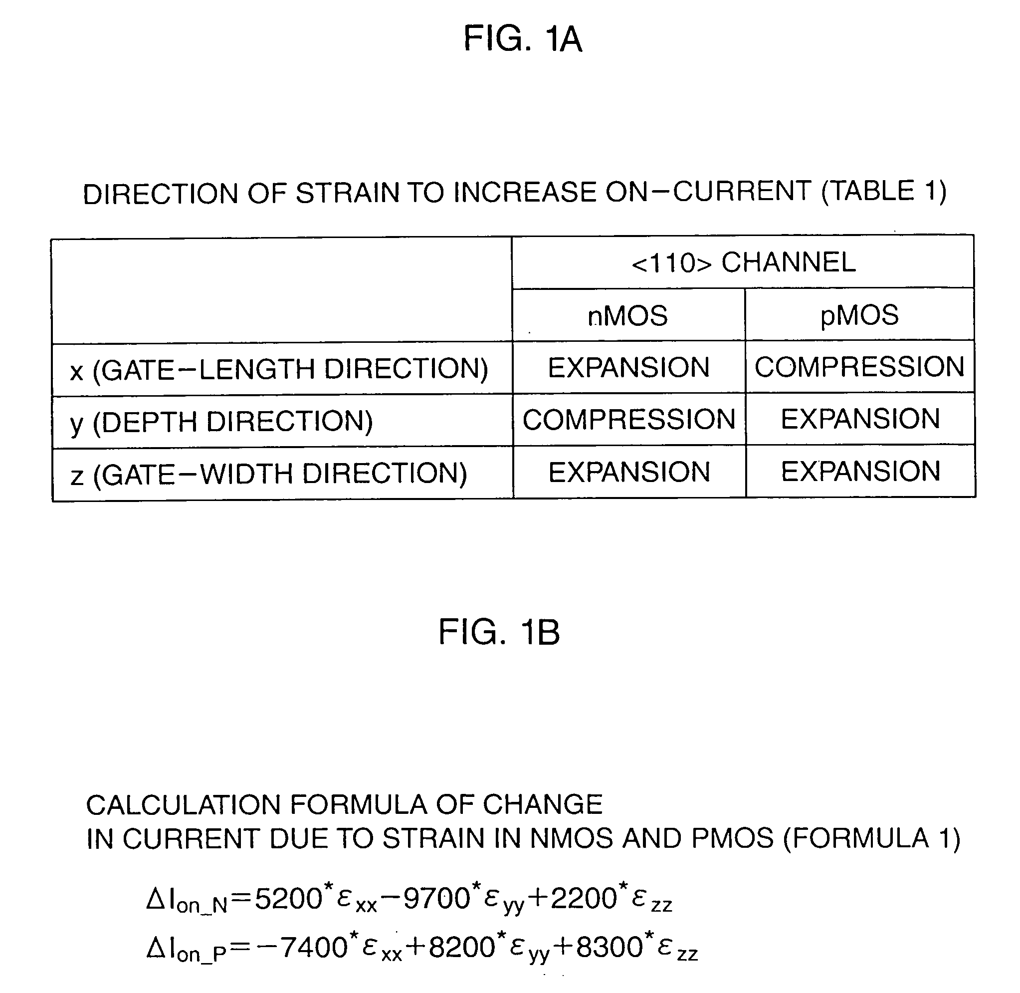
a technology of semiconductor devices and semiconductors, applied in the field of semiconductor devices, can solve the problems of many difficulties in technique and manufacturing cost realization, increase in process and process complexity, and decrease in on-current of sti element isolation structures, so as to reduce stress efficiently, improve on-current, and reduce gate-width direction dependence

Inactive Publication Date: 2006-10-05
FUJITSU SEMICON LTD
View PDF25 Cites 0 Cited by
  • Summary
  • Abstract
  • Description
  • Claims
  • Application Information

AI Technical Summary

Benefits of technology

[0015] As described above, when the STI element isolation structure is used, a device structure with less gate-width direction dependence of the stress is demanded to relive the stress applied to the active region and efficiently reduce the stress, in order to improve the on-current. Presently, a technology is being sought which easily and surely meets these two demands without causing an increase in processes and complication of processes.
[0016] The present invention has been developed in consideration of the above problems and its object is to provide a reliable semiconductor device having excellent current characteristics in a semiconductor device including the STI element isolation structure in which the gate-width direction dependence of the stress is significantly reduced and the stress applied to the active regions is relieved easily and surely without causing an increase in processes and complication of processes, and a method of manufacturing the same.

Problems solved by technology

However, the use of the STI element isolation structure suffers from a decrease in on-current due to stress on the active region applied from the STI element isolation structure.
In this case, however, the N-type MOS transistor and the P-type MOS transistor are formed by different processes, thus necessarily leading to increase in processes and complication of processes, and in addition, they need to be formed using materials which have not conventionally been used, to encounter many difficulties in technique and manufacturing cost for realization.

Method used


Image

  • Semiconductor device and method of manufacturing the same
  • Semiconductor device and method of manufacturing the same
  • Semiconductor device and method of manufacturing the same

Examples


first embodiment

[0038] -First Embodiment-

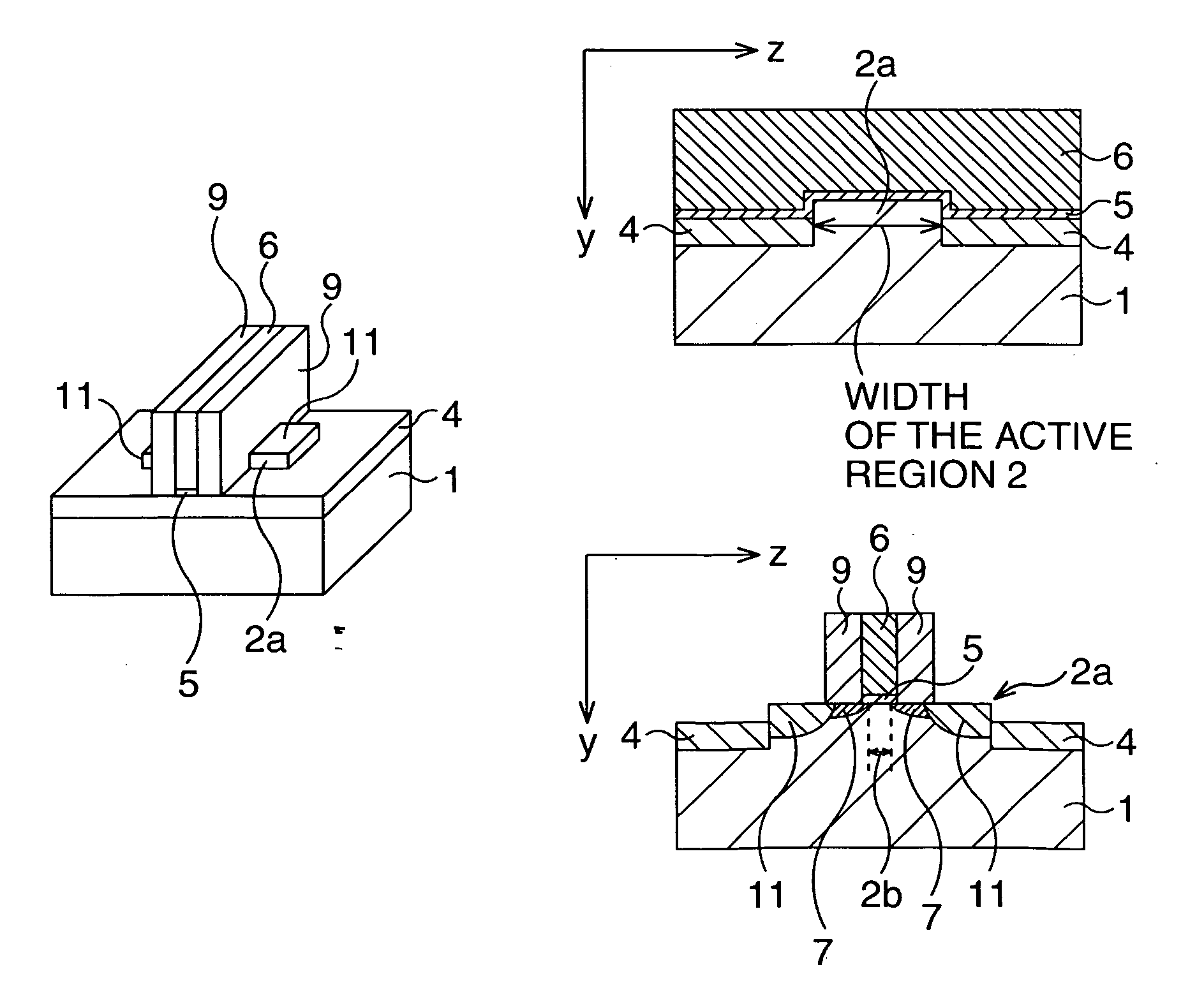
[0039]FIGS. 3A to 3C are schematic perspective views showing main processes in a method of manufacturing a CMOS transistor according to the first embodiment selected only for the P-type MOS transistor, and FIG. 3C that is a completion view of the P-type MOS transistor additionally shows schematic cross-sectional views along a z-y plane and an x-y plane of the transistor. FIGS. 4A to 4F are schematic cross-sectional views showing the method of manufacturing the CMOS transistor according to the first embodiment in the order of processes, each view corresponding to a schematic cross section along the x-y plane shown in FIG. 3C.

[0040] First, as shown in FIG. 3A and FIG. 4A, on a silicon substrate 1, an active region 2 of the P-type MOS transistor and an active region 3 of the N-type MOS transistor are defined, respectively.

[0041] More specifically, element isolation structures are formed respectively within the element isolation region for the P-type MOS trans...

modification example -

[0060] -Modification Example-

[0061] Here, a modification example of the first embodiment will be described. In this modification example, a CMOS transistor is manufactured as in the first embodiment, but is different in that a process is added which relieves the stress of the STI element isolation structure 4 by introduction of an element.

[0062]FIGS. 5A and 5B are schematic views showing processes added to the first embodiment in this modification example, and FIG. 5A is a schematic plan view and FIG. 5B is a schematic cross-sectional view along a broken line I-I in FIG. 5A.

[0063] First, processes in FIGS. 4A and 4B (FIGS. 3A and 3B) are performed.

[0064] Subsequently, as shown in FIGS. 5A and 5B, a resist mask 13 covering the active region 2 and extending in the x-direction is formed only within the active region 2 for the P-type MOS transistor.

[0065] More specifically, a resist is applied over the entire surface and processed by lithography to thereby form the resist mask 13 on...

second embodiment

[0073] -Second Embodiment-

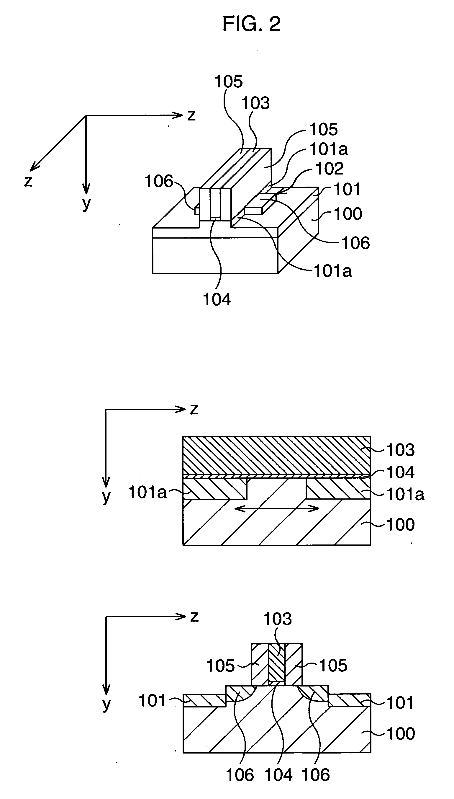
[0074]FIGS. 6A to 6C are schematic views showing main processes in a method of manufacturing a CMOS transistor according to the second embodiment selected only for the P-type MOS transistor. The left drawing is a schematic perspective view and the right drawing is a schematic plan view in each of FIGS. 6A and 6B, and FIG. 6C illustrates a schematic plan view of a completion view of the P-type MOS transistor showing the state in which its gate insulation film, gate electrode, and side wall spacers are removed therefrom. In the drawings of FIGS. 6A to 6C, the numerals and symbols of components and so on associated with the N-type MOS transistor are shown in parentheses. FIGS. 7A to 7E are schematic cross-sectional views showing the method of manufacturing the CMOS transistor according to the second embodiment in the order of processes, each view corresponding to a schematic cross section along an x-y plane shown in FIGS. 6A to 6C. Note that the same numerals ...


PUM


Abstract

Each of channel regions 2a and 3b is covered by a gate electrode 6 via a gate insulation film 5 and side wall spacers 9 from its top face to both side faces along an x-direction. In other words, there is no insulation material of an STI element isolation structure 4 on both side faces along the x-direction of each of the channel regions 2b and 3b (in a non-contact state), thereby preventing stress in a z-direction from being applied by the STI element isolation structure 4 to each of the channel region 2b and 2b.

Description

CROSS-REFERENCE TO RELATED APPLICATIONS [0001] This application is based upon and claims the benefit of priority from the prior Japanese Patent Application No. 2005-096093, filed on Mar. 29, 2005, the entire contents of which are incorporated herein by reference. BACKGROUND OF THE INVENTION [0002] 1. Field of the Invention [0003] The present invention relates to a semiconductor device having an element isolation structure by the STI (Shallow Trench Isolation) method and a method of manufacturing the same. [0004] 2. Description of the Related Art [0005] Conventionally, as an element isolation structure, an element isolation structure formed by the STI method (hereinafter, simply referred to as an STI element isolation structure) has been used in which insulation within an active region is ensured by embedding an insulation material in a groove formed within the element isolation region. This STI element isolation structure is expected to contribute to demands for miniaturization of s...

Claims


Application Information

Patent Timeline
Patent Type & Authority Applications(United States)
IPC IPC(8): H01L21/336
CPCH01L21/823807H01L29/78H01L29/6659H01L21/823878
Inventor TANABE, RYO
Owner FUJITSU SEMICON LTD
Why Eureka
Try Eureka