Self-aligned contacts for transistors

a technology of self-aligning contacts and transistors, which is applied in the direction of transistors, semiconductor devices, electrical equipment, etc., can solve the problems of low self-alignment, low self-alignment, and high external electrical resistance (“rext”),

Active Publication Date: 2006-10-05
DAEDALUS PRIME LLC
View PDF61 Cites 314 Cited by
  • Summary
  • Abstract
  • Description
  • Claims
  • Application Information

AI Technical Summary

Problems solved by technology

One of the problems associated with certain prior art trigate transistors and nanowire devices is that external electrical resistance (“Rext”) can sometimes be relatively high.
Misalignment problems with contacts can lead to variations in Rext for the various trigate transistors, however, leading to less predicatability with respect to the design and performance of the overall integrated circuit.
This can result in transistor mismatches.
One problem with that prior art approach, however, is that it is difficult to make a large enough area for a contact using epitaxial growth on a small silicon area—i.e., there is not much silicon to work with.
The prior art landing pad approach can be problematic, however.
Due to lithography constraints, the prior art landing pads typically must lie relatively far from the gate of the transistor.
The thin silicon body of the diffusion layer and diffusion jog between the contact and the gate typically results in high external electrical resistance.
Moreover, the landing pads can create undersirable jogs, sometimes causing problems for optical lithography, especially for sub-100 nanometer (“nm”) devices.
External electrical resistance problems can occur on devices beside trigate transistors.
In principle, any transistor with a thin diffusion can have an Rext problem.
There can be Rext problems even on bulk devices on 65 nanometer nodes.

Method used


Image

  • Self-aligned contacts for transistors
  • Self-aligned contacts for transistors
  • Self-aligned contacts for transistors

Examples


Embodiment Construction

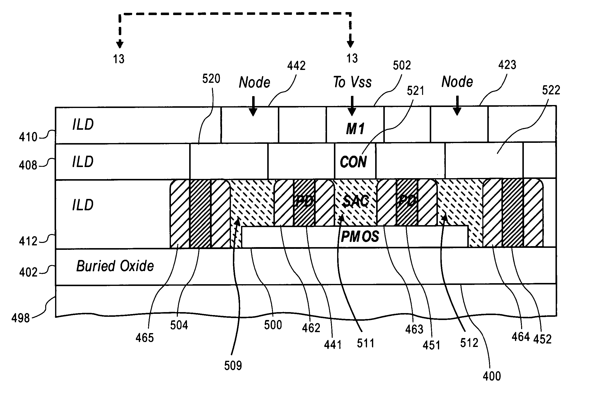
[0036] Embodiments of self-aligned contacts are described as well as methods for fabricating such contacts.

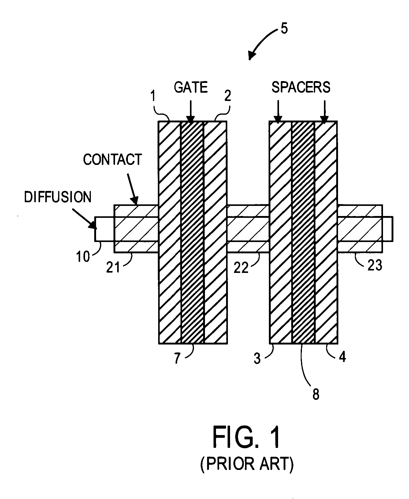
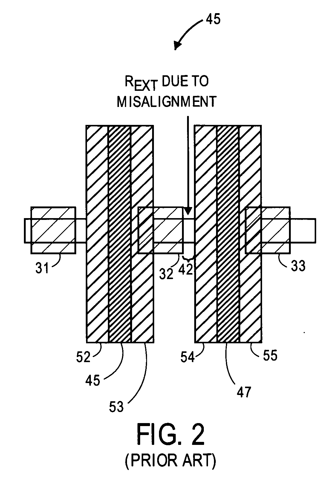
[0037] As described in more detail below, a self-aligned contact (“SAC”) brings the contact physically all the way to a spacer associated with a gate of a transistor. This arrangement can help to minimize electrical external resistance (“Rext”) associated with a thin and long diffusion body of the transistor. The minimization (or elimination) of Rext can also minimize (or eliminate) variations of Rext. Variations in Rext can cause transistor mismatches.

[0038] For one embodiment, superadjacent contacts reside in a layer above the self-aligned contacts and provide respective electrical connections to the self-aligned contacts. The self-aligned contacts have a relatively wide top surface layer and the superadjacent contacts have smaller horizontal cross sections than the respective self-aligned contacts. This means that the superadjacent contacts do not have to be precisely alig...


PUM


Abstract

Self-aligned contacts for transistors and methods for fabricating the contacts are described. An etch resistant material is patterned to create an opening that resides above a transistor gate structure. A selective etch is performed through the opening that does not etch the transistor gate structure but does etch material that resides laterally with respect to the transistor gate structure in order to expose tops, immediately adjacent to the transistor gate structure, of drain and source regions of a diffusion layer of the transistor. Conductive material is deposited that covers respective tops of the drain and source regions of the diffusion layer of the transistor to a depth that does not short the drain and source region of the diffusion layer of the transistor. A layer above the conductive material is formed. Contacts are formed through the layer above the conductive material to respective portions of the conductive material that cover respective tops of the drain and source regions of the diffusion layer of the transistor.

Description

FIELD [0001] Embodiments of the invention relate to semiconductor layout and fabrication. In particular, embodiments of the invention relate to self-aligned contacts for transistors and methods for fabricating the contacts. BACKGROUND [0002] Trigate transistors and nanowire devices (i.e., transistors having bodies made from nanowires) typically have small geometries. For trigate transistors, the diffusion regions and the gates are typically quite thin. [0003]FIG. 1 illustrates a properly-aligned prior art trigate transistor structure 5 comprised of two trigate transistors having respective gates 7 and 8 and a common diffusion region 10. Spacers 1 and 2 are adjacent to gate 7. Spacers 3 and 4 are adjacent to gate 8. Metallic contacts 21, 22, and 23 provide electrical contacts to diffusion region 10. [0004] One of the problems associated with certain prior art trigate transistors and nanowire devices is that external electrical resistance (“Rext”) can sometimes be relatively high. Hig...

Claims


Application Information

Patent Timeline
Patent Type & Authority Applications(United States)
IPC IPC(8): H01L21/4763
CPCH01L21/76897H01L21/84H01L27/1203H01L27/1108H01L27/11H10B10/125H10B10/00
Inventor CHANG, PETER L.D.DOYLE, BRIAN S.
Owner DAEDALUS PRIME LLC
Why Eureka
Try Eureka