Plating apparatus, plating method, and method for manufacturing semiconductor device

a technology of plating apparatus and semiconductor device, which is applied in the manufacture of electrolysis components, tanks, manufacturing tools, etc., can solve the problems of oxidative decomposition of additive agents contained in the plating solution, easy peeling of black film on the surface of the anode electrode, and degrading the quality of the plating, etc., to maintain the operability of the apparatus.

Inactive Publication Date: 2006-10-12
SHARP KK
View PDF9 Cites 29 Cited by
  • Summary
  • Abstract
  • Description
  • Claims
  • Application Information

AI Technical Summary

Benefits of technology

[0020] In view of the above problems, the present invention has as an object to provide (i) a plating apparatus, especially a face-down type fountain plating apparatus, with which the plating quality would not be degr

Problems solved by technology

The face-down type fountain plating apparatus has a problem in that micro foreign solid particles adhere to the plating-target face, and therefore the plating quality is degraded.
This problem is originated from the surface of the anode electrode in the path through which the plating solution streams; the plating solution supplied from the plating solution storage tank by the pump is filtrated by the filter, is supplied to the cup from the underneath thereof, passes by the vicinity of the anode electrode, and reaches the plating-target face of the semiconductor wafer.
However, the black film formed on the surface of the anode electrode is easily peeled off therefrom.
This causes a problem in that the black film adheres to a plat

Method used


Image

  • Plating apparatus, plating method, and method for manufacturing semiconductor device
  • Plating apparatus, plating method, and method for manufacturing semiconductor device
  • Plating apparatus, plating method, and method for manufacturing semiconductor device

Examples


first embodiment

[0059] The following describes one embodiment of the present invention, with reference to FIGS. 1 to 8(a) and 8(b).

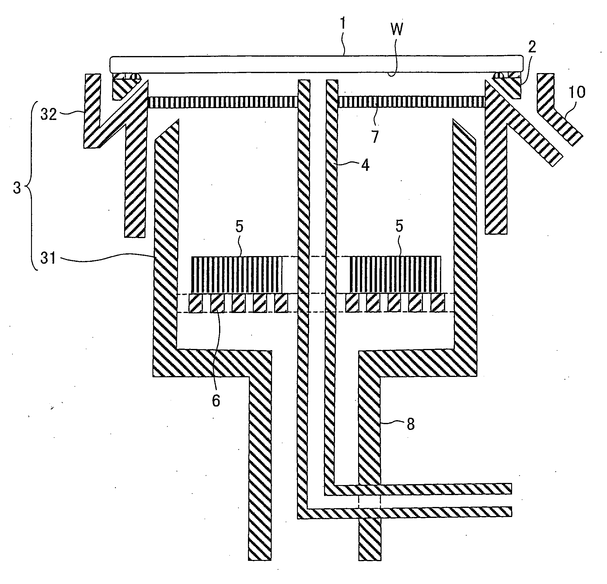
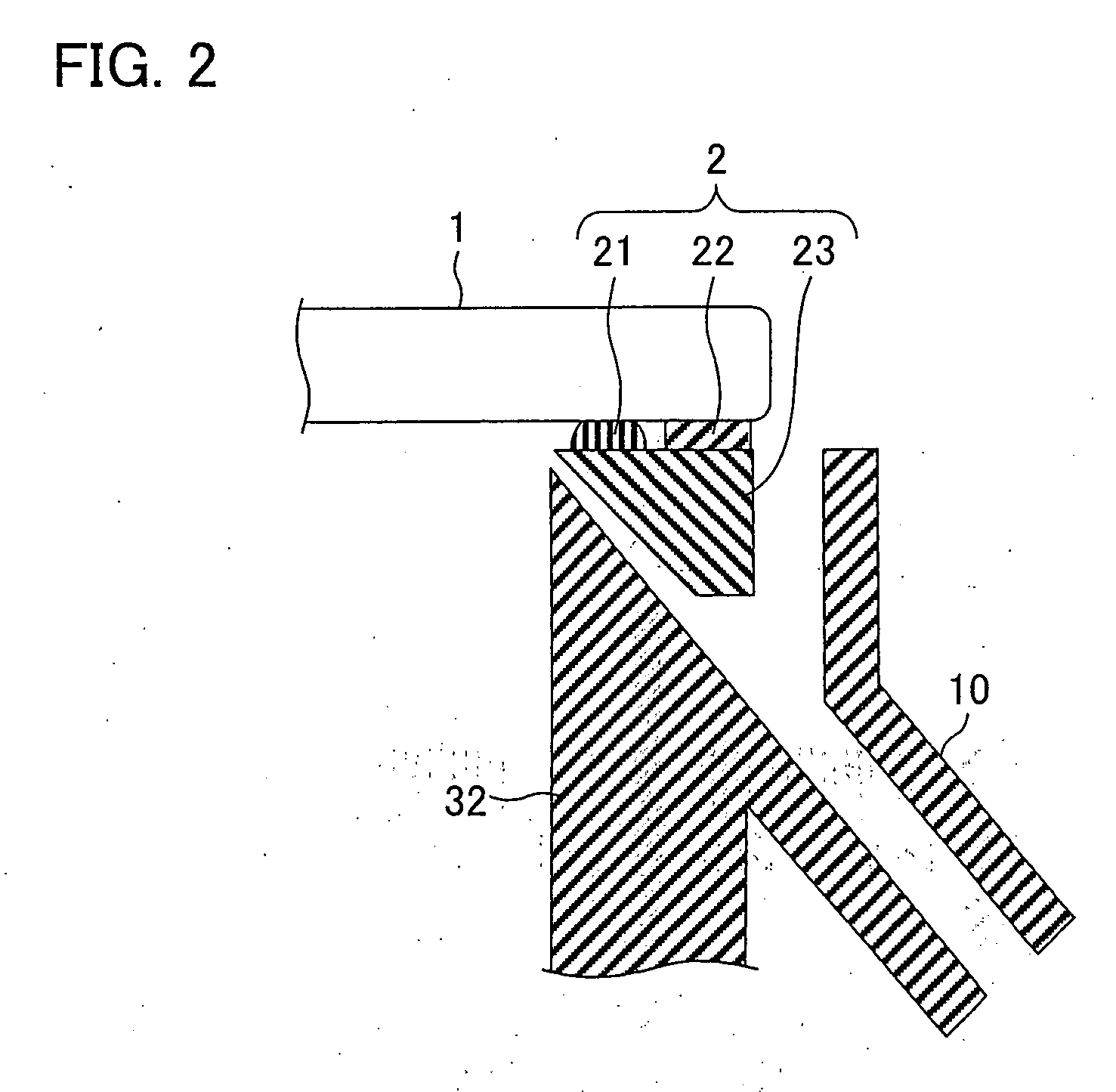
[0060]FIG. 1 is a cross sectional diagram schematically illustrating a structure of a plating tank provided to a plating apparatus of the present embodiment. As illustrated in FIG. 1, a plating tank 100 is provided with: a wafer holder 2 that holds a semiconductor wafer (plating-target substrate (substrate to be plated)) 1; a cup 3; a plating solution supply nozzle (plating solution jet tube) 4; an anode electrode 5; a supporting member 6 that supports the anode electrode 5; a partition 7; and an electrolytic liquid supply tube 8. The cup 3 is provided with an inner tube 31 and an outer tube 32.

[0061] The inner tube (second cylinder cup) 31 and the outer tube (first cylinder cup) 32 are containers each having a substantially cylindrical shape with an opening top. The outer diameter of the inner tube 31 is so designed as to be smaller than that of the outer tube 32. Th...

second embodiment

[0124] The following describes another embodiment according to the present invention, with reference to FIGS. 9 and 10. In the present embodiment, the differences between the present embodiment and the first embodiment described above will be explained. Therefore, for the purpose of convenience, the members having the same functions as those explained in the first embodiment are given the same reference numerals, and explanations thereof are omitted.

[0125]FIG. 9 is a cross sectional diagram schematically illustrating a structure of a plating tank provided to the plating apparatus of the present embodiment. As illustrated in FIG. 9, the plating tank 200 is provided with: a wafer holder 2 that holds a semiconductor wafer (plating-target substrate (face to be plated)) 1; a cup 3; a plating solution supply nozzle 4; an anode electrode 5; a supporting member 6 that supports the anode electrode 5; a partition 7; an electrolytic liquid supply tube 8; an upper covering member 28; and an O-...

third embodiment

[0179] In the present embodiment, a method for manufacturing a semiconductor chip using a plating apparatus according to one of the first or the second embodiments will be explained in detail, with reference to FIGS. 13(a) to 13(g), and FIGS. 14(a) to 14(d). FIG. 13 are cross sectional diagram illustrating the process of the method for manufacturing a semiconductor device according to the present embodiment. In the present embodiment, as one example of the method for manufacturing a semiconductor device, a method for manufacturing the semiconductor chip 41 illustrated in FIGS. 7, 8(a), and 8(b) will be explained.

[0180] As illustrated in FIGS. 13(a) to 13(g), the method for manufacturing the semiconductor device according to the present embodiment includes the steps of: forming a seed layer 19 on the surface of the semiconductor chip 41; applying a photoresist on the seed layer 19 thereby to form a photoresist layer 18 thereon; forming an arbitrary pattern on the photoresist layer 1...


PUM

PropertyMeasurementUnit
Massaaaaaaaaaa
Massaaaaaaaaaa
Volumeaaaaaaaaaa

Abstract

A plating apparatus according to the present invention is provided with a plating tank 100 in which an anode electrode 5 is provided, the plating apparatus performing the plating by (i) streaming a plating solution and an electrolytic liquid into the plating tank 100, (ii) emitting a jet of the plating solution to the plating-target face W of the semiconductor wafer 1 from the underneath of the semiconductor wafer 1, and (iii) streaming the electrolytic liquid to the anode electrode 5 while electrically conducting between the semiconductor wafer 1 and the anode electrode 5, the plating tank including a partition in between the semiconductor wafer 1 and the anode electrode 5, and the partition (i) separating the semiconductor wafer 1 and the anode electrode 5 and (ii) dividing the plating tank 100 into a plating-target substrate room and an anode electrode room. Thus, in a face-down type fountain plating apparatus, the plating quality would not be degraded by micro foreign solid particles originated from, for example, a black film while maintaining the operability of the apparatus.

Description

[0001] This Nonprovisional application claims priority under 35 U.S.C. §119(a) on Patent Applications (i) No. 112888 / 2005 filed in Japan on Apr. 8, 2005 and (ii) No. 202283 / 2005 filed in Japan on Jul. 11, 2005, the entire contents of which are hereby incorporated by reference. FIELD OF THE INVENTION [0002] The present invention relates to (i) a plating apparatus, (ii) a plating method, and (iii) a method for manufacturing a semiconductor device, all of which are excellent for finely plating a plating-target face of, for example, a semiconductor wafer in order to form wiring. BACKGROUND OF THE INVENTION [0003] In the recent years, metal plating has been utilized for forming a wiring on, for example, a semiconductor wafer. Known conventional apparatuses utilized for metal plating include a face-down type fountain plating apparatus, a rack-method vertical plating apparatus, and a face-up type fountain plating apparatus. [0004] The face-down type fountain plating apparatus, as illustrat...

Claims


Application Information

Patent Timeline
IPC IPC(8): C25D5/20C25B9/00
CPCC25D5/08C25D17/008C25D17/002C25D17/001C25D7/123H01L2224/11C25D17/00C25D17/02
Inventor IWAZAKI, YOSHIHIDE
Owner SHARP KK
Why Eureka
Try Eureka