Nitride-based semiconductor light emitting device and manufacturing method thereof

Inactive Publication Date: 2006-10-12
SHARP KK
View PDF27 Cites 29 Cited by
  • Summary
  • Abstract
  • Description
  • Claims
  • Application Information

AI Technical Summary

Benefits of technology

[0013] According to the present invention, a highly reliable light emitting device where adhesion between the nitrid

Problems solved by technology

However, since the entire surface of the conductive substrate of a large area and the entire surface of the nitride-based semiconductor layer are bonded together via the ohmic electrode and bonding metal, it has been difficult to apply uniform heating and pressure bonding.
As such, there has been a problem that the entire surface of the nitride-based semiconductor layer may peel off from the conductive substrate due to poor adhesion therebetween.
If the ohmic electrode and the bonding metal are separated from the conductive substrate completely, it is not possible to remove a sapphire substrate used as a base substrate, which hinders formation of a nitride-based semiconductor light emitting device having electrodes on both main surfaces.
There has been a problem that, if the conductive substrate and the nitride-based semiconductor l

Method used


Image

  • Nitride-based semiconductor light emitting device and manufacturing method thereof
  • Nitride-based semiconductor light emitting device and manufacturing method thereof
  • Nitride-based semiconductor light emitting device and manufacturing method thereof

Examples


first embodiment

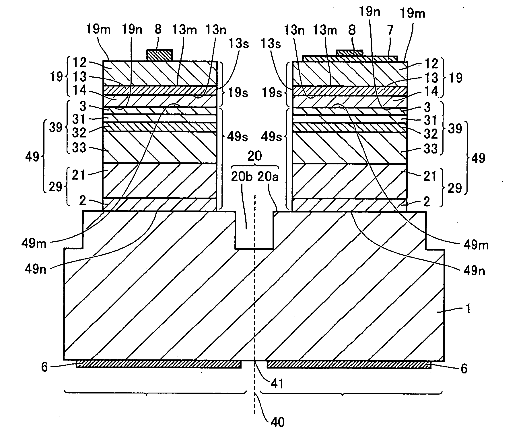
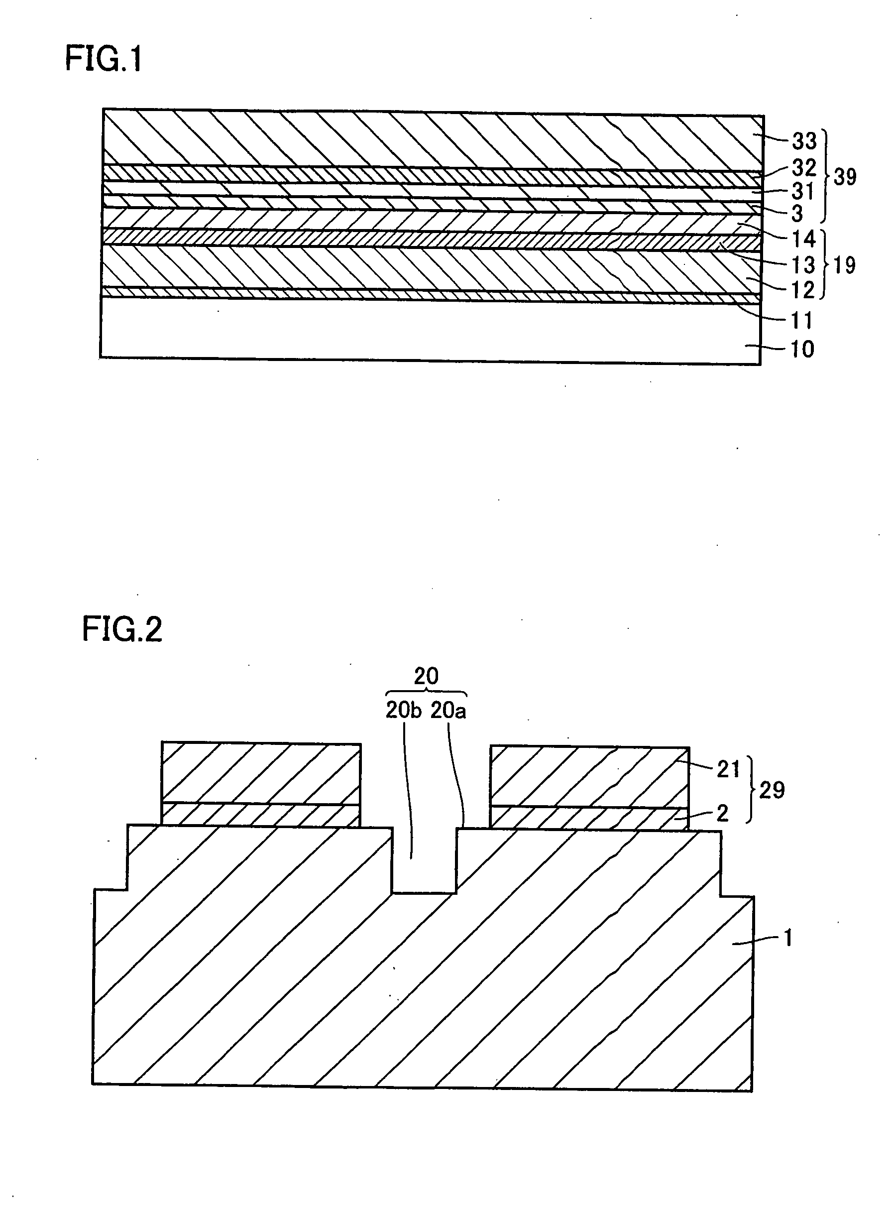
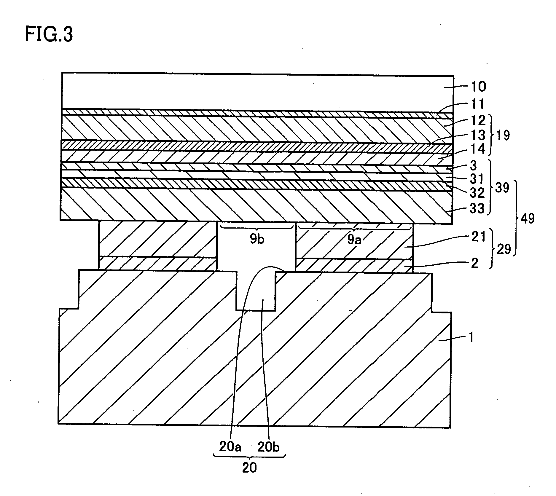
[0042] Referring to FIG. 6, a nitride-based semiconductor light emitting device 60 in an embodiment of the present invention has a pattern surface 20a formed on an Si substrate serving as conductive substrate 1, on which a multilayered metal layer 49 and a multilayered semiconductor layer 19 having main surfaces 49m, 49n, 19m, and 19n having smaller area than pattern surface 20a has are formed. Here, multilayered metal layer 49 is constituted by a substrate-side multilayered metal layer 29 including an ohmic electrode 2 and a bonding metal layer 21 formed on pattern surface 20a of conductive substrate 1, and a semiconductor-side multilayered metal layer 39 including a bonding metal layer 33, a barrier layer 32, a reflection metal layer 31 and an ohmic electrode 3, wherein bonding metal layer 21 of substrate-side multilayered metal layer 29 and bonding metal layer 33 of semiconductor-side multilayered metal layer 39 are joined. On ohmic electrode 3 of semiconductor-side multilayered ...

second embodiment

[0052] Referring to FIG. 7, a nitride-based semiconductor light emitting device 70 in another embodiment of the present invention has a pattern surface 20a formed on an Si substrate serving as conductive substrate 1, on which a multilayered metal layer 49 and a multilayered semiconductor layer 19 having main surfaces 49m, 49n, 19m, and 19n having smaller area than pattern surface 20a has are formed. Here, multilayered metal layer 49 is constituted by a substrate-side multilayered metal layer 29 including an ohmic electrode 2 and a bonding metal layer 21 formed on pattern surface 20a of conductive substrate 1, and a semiconductor-side multilayered metal layer 39 including a bonding metal layer 33, a barrier layer 32, a reflection metal layer 31 and a ohmic electrode 3, wherein bonding metal layer 21 of substrate-side multilayered metal layer 29 and bonding metal layer 33 of semiconductor-side multilayered metal layer 39 are joined. On ohmic electrode 3 of semiconductor-side multilaye...


PUM


Abstract

A present nitride-based semiconductor light emitting device includes: a pattern surface formed on a conductive substrate; a multilayered metal layer formed on the pattern surface; and a multilayered semiconductor layer formed on the multilayered metal layer, and characterized in that main surfaces of the multilayered metal layer and the multilayered semiconductor layer have smaller area than the pattern surface has, and the multilayered semiconductor layer includes a p type nitride-based semiconductor layer, a light emitting layer and an n type nitride-based semiconductor layer. Thus, a highly reliable nitride-based semiconductor light emitting device with excellent adhesion between a nitride-based semiconductor layer and a conductive substrate, and a manufacturing method thereof are provided.

Description

[0001] This nonprovisional application is based on Japanese Patent Applications Nos. 2005-114386 and 2006-042630 filed with the Japan Patent Office on Apr. 12, 2005 and Feb. 20, 2006, respectively, the entire contents of which are hereby incorporated by reference. BACKGROUND OF THE INVENTION [0002] 1. Field of the Invention [0003] The present invention relates to a nitride-based semiconductor light emitting device such as a semiconductor laser diode or a light emitting diode and to a manufacturing method thereof, and particularly to a manufacturing method of a nitride-based semiconductor light emitting device including a step of bonding a patterned conductive substrate and a multilayered semiconductor layer including a nitride-based semiconductor layer and to a nitride-based semiconductor light emitting device obtained by the manufacturing method. [0004] 2. Description of the Background Art [0005] A conventional nitride-based semiconductor light emitting device is formed as shown in...

Claims


Application Information

Patent Timeline
IPC IPC(8): H01L33/00H01L33/06H01L33/12H01L33/32H01L33/34H01L33/42
CPCH01L33/0079H01L33/32H01L33/20H01L33/0093
Inventor HATA, TOSHIO
Owner SHARP KK
Why Eureka
Try Eureka