Method for forming a porous polishing pad

a technology of polishing pads and porous surfaces, applied in the field of polishing pads, can solve the problems of unpredictability, perhaps detrimental, polishing performance, detrimental to polishing performance, etc., and achieve the effect of improving polishing performance and polishing performan

Active Publication Date: 2006-10-12
ROHM & HAAS ELECTRONICS MATERIALS CMP HLDG INC
View PDF15 Cites 41 Cited by
  • Summary
  • Abstract
  • Description
  • Claims
  • Application Information

AI Technical Summary

Benefits of technology

[0007] Hence, what is needed is a polishing pad having improved polishing performance. Moreover, what is needed is an apparatus and an efficient method of forming a porous polishing pad having improved polishing performance.

Problems solved by technology

Unfortunately, polishing pads of Hishiki have large variations in porosity and may cause unpredictable, and perhaps, detrimental, polishing performances from one polishing pad to the next.
In other words, these polishing pads have variations in porosity of up to about 80 percent, which may detrimentally affect polishing performance.
Moreover, these variations in porosity may negatively affect polishing performance within the pad itself.

Method used


Image

  • Method for forming a porous polishing pad
  • Method for forming a porous polishing pad
  • Method for forming a porous polishing pad

Examples


Embodiment Construction

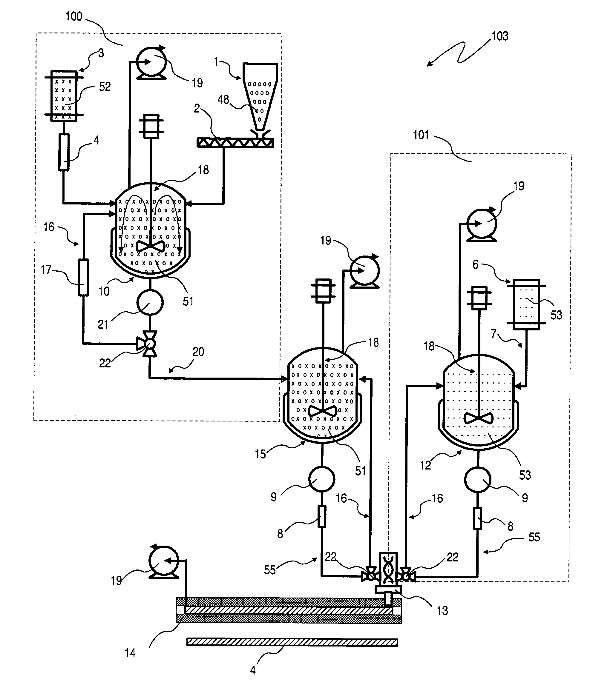
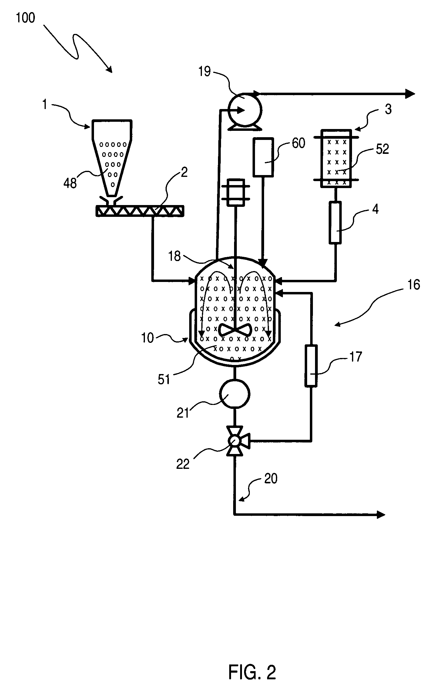
[0022] The present invention provides a porous polishing pad. Further, the present invention provides a novel apparatus and method for forming a porous polishing pad by the in-situ expansion of fluid-filled unexpanded microspheres. In particular, the present invention utilizes a unique premix apparatus to produce the porous polishing pad in, for example, an injection-reaction molding or casting process. The premix apparatus comprises, a novel premix prep tank for pre-mixing the unexpanded microspheres and the polymeric materials (e.g., polyols or prepolymers) to form a homogeneous pre-mixture. The premix apparatus may further comprise a vacuum to remove or degas any mechanically entrained or dissolved gas. In addition, the novel apparatus provides tremendous flexibility in increasing manufacturing scale and in pad-type variation. In other words, the novel apparatus allows, for example, continuous reaction-injection molding or casting and the use of almost an endless combination of d...


PUM

PropertyMeasurementUnit
average cell diameteraaaaaaaaaa

Abstract

The present invention provides a method of forming a chemical mechanical polishing pad comprising providing a polymeric matrix with fluid-filled unexpanded microspheres, curing the polymeric matrix and heating the polymeric matrix and the microspheres to expand the microspheres.

Description

CROSS REFERENCE TO RELATED APPLICATION [0001] This application claims the benefit of U.S. Provisional Application Ser. No. 60 / 670,361 filed Apr. 11, 1005.BACKGROUND OF THE INVENTION [0002] The present invention relates to polishing pads for chemical mechanical planarization, and in particular, relates to porous polishing pads. Further, the present invention relates to apparatuses and methods for forming porous polishing pads formed from unexpanded microspheres. [0003] In the fabrication of integrated circuits and other electronic devices, multiple layers of conducting, semiconducting and dielectric materials are deposited on or removed from a surface of a semiconductor wafer. Thin layers of conducting, semiconducting, and dielectric materials may be deposited by a number of deposition techniques. Common deposition techniques in modern processing include physical vapor deposition (PVD), also known as sputtering, chemical vapor deposition (CVD), plasma-enhanced chemical vapor depositi...

Claims


Application Information

Patent Timeline
Patent Type & Authority Applications(United States)
IPC IPC(8): B29C44/06
CPCB24D11/001B29C70/66B29B7/90B29B7/749B29B7/726B29B7/7471B29B7/748B29B7/7485
Inventor JAMES, DAVID B.KULP, MARY JOROBERTS, JOHN V.H.
Owner ROHM & HAAS ELECTRONICS MATERIALS CMP HLDG INC
Why Eureka
Try Eureka