Anti-eclipse circuitry with tracking of floating diffusion reset level

Active Publication Date: 2006-10-12
MICRON TECH INC
View PDF11 Cites 18 Cited by
  • Summary
  • Abstract
  • Description
  • Claims
  • Application Information

AI Technical Summary

Benefits of technology

[0018] Since the anti-eclipse circuit is affected by the same fabrication processing conditions as the imaging array pixels and

Problems solved by technology

Unfortunately, semiconductor fabrication pr

Method used


Image

  • Anti-eclipse circuitry with tracking of floating diffusion reset level
  • Anti-eclipse circuitry with tracking of floating diffusion reset level
  • Anti-eclipse circuitry with tracking of floating diffusion reset level

Examples


Embodiment Construction

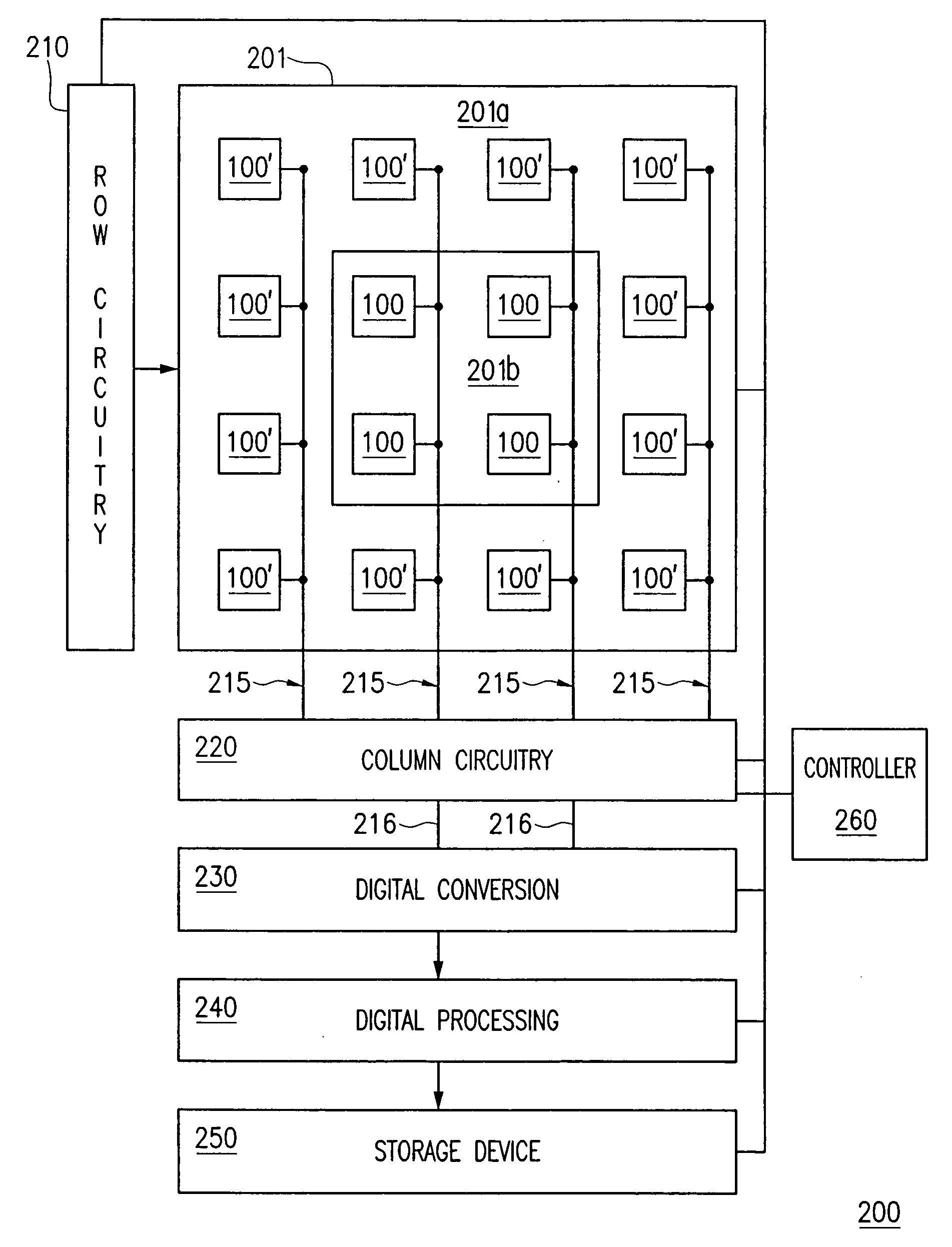
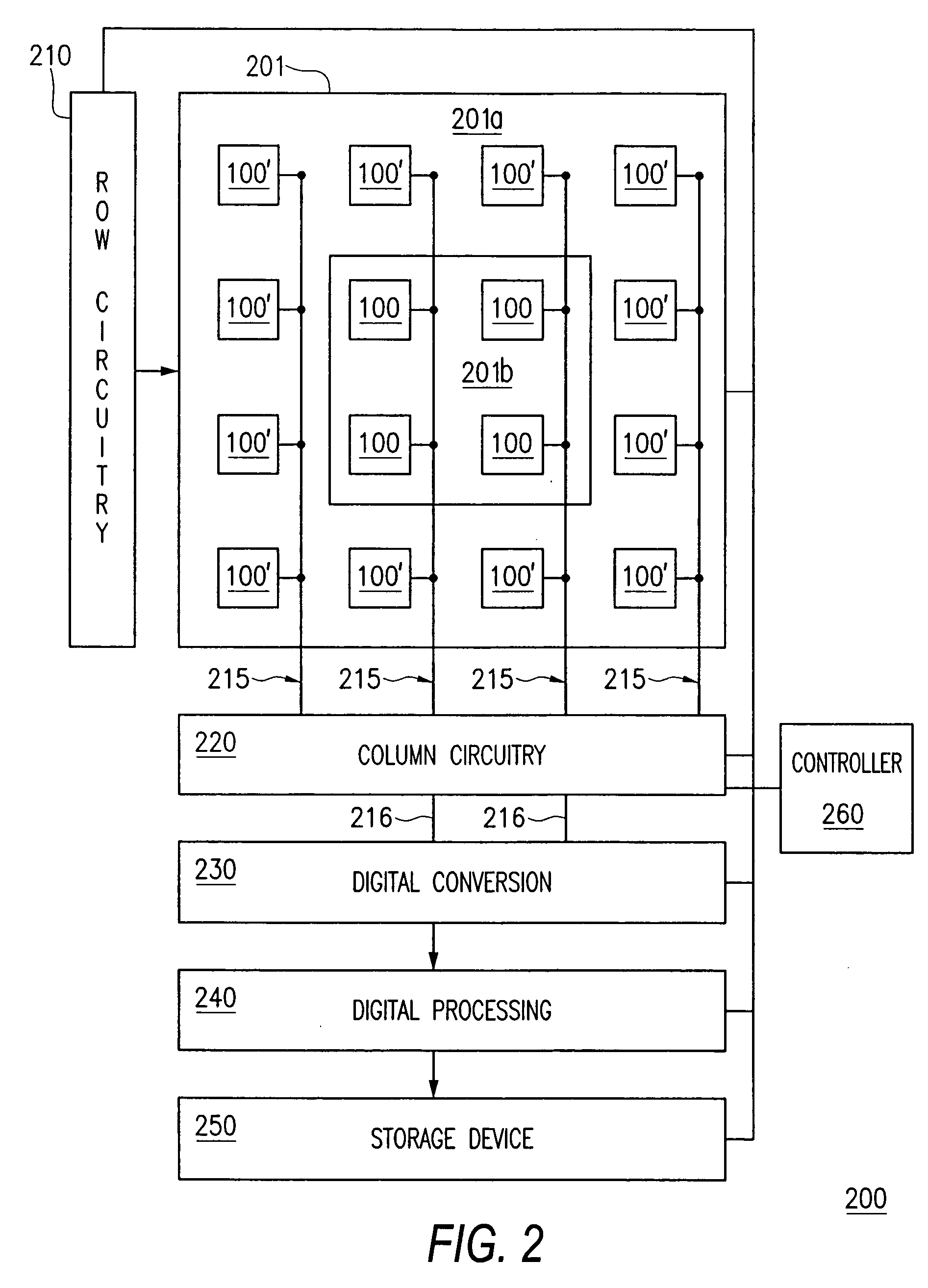
[0028] Now referring to the drawings, where like reference numerals designate like elements, there is shown in FIG. 6 is an illustration of a circuit 600 for generating the anti-eclipse threshold voltage AE_Vref in accordance with an exemplary embodiment of the invention. The circuit 600 is preferably formed on the same integrated circuit as at least the pixel array 201 and column circuit 220 of an associated imager, but is not otherwise part of the array of pixels generating image signals. The circuit 600 generates the anti-eclipse threshold voltage AE_Vref for each of the anti-eclipse circuits 310 (FIG. 3) of an imager 200. As explained in greater detail below, portions of the circuit 600 are modifications of pixel circuits (e.g., a non-image pixels whose output would not be further processed). By utilizing modified pixel circuits on the same integrated circuit as the pixel array and the column circuit 220, the circuit 600 is subject to the same semiconductor fabrication induced v...


PUM


Abstract

An anti-eclipse circuit for an imager is formed from pixel circuitry over the same semiconductor substrate as the imaging pixels. More specifically, two adjacent pixel circuits are modified to form an amplifier. One input of the amplifier is adapted to receive a reset signal from one of the pixel circuits while another input is adapted to be set at a predetermined offset voltage from the output of the amplifier. The amplifier is preferably a unity gain amplifier, so that the output of the amplifier set to a voltage level equal to the predetermined offset from the voltage level of the reset signal. Accordingly, the anti-eclipse circuit outputs a reference voltage at predetermined level from the reset voltage of a pixel and does not need to be calibrated for fabrication related variances in reset voltages.

Description

FIELD OF INVENTION [0001] The present invention relates generally to pixel architectures for semiconductor imagers. More specifically, the present invention relates to an anti-eclipse system for image sensors. BACKGROUND OF THE INVENTION [0002]FIG. 1 is an illustration of a conventional four transistor (4T) pixel 100. The pixel 100 includes a light sensitive element 101, shown as a photodiode, a floating diffusion node C, and four transistors: a transfer transistor 111, a reset transistor 112, a source follower transistor 113, and a row select transistor 114. The pixel 100 accepts a TX control signal for controlling the conductivity of the transfer transistor 111, a RST control signal for controlling the conductivity of the reset transistor 112, and a ROW control signal for controlling the conductivity of the row select transistor 114. The voltage at the floating diffusion node C controls the conductivity of the source follower transistor 113. The output of the source follow transis...

Claims


Application Information

Patent Timeline
IPC IPC(8): H04N5/217
CPCH04N5/3598H04N5/3742H04N5/361H04N5/3653H04N25/627H04N25/672H04N25/77H04N25/63H04N25/767
Inventor OLSEN, ESPEN A.
Owner MICRON TECH INC
Why Eureka
Try Eureka