Patterned material layer, method of forming the same, microdevice, and method of manufacturing the same

Inactive Publication Date: 2006-10-12
TDK CORPARATION
View PDF3 Cites 4 Cited by
  • Summary
  • Abstract
  • Description
  • Claims
  • Application Information

AI Technical Summary

Benefits of technology

[0005] Methods forming a material layer by vacuum coating can easily turn various materials into thin films and can employ a wide range of materials. In the case of magnetic materials, for example, these methods are also advantageous in that they yield material layers with a saturated magnetic flux density higher than that in material layers formed by frame plating.
[0007] In view of the foregoing circumstances, it is an object of the present invention to provide a method of forming a patterned material layer which can pattern a material layer formed on a substrate by vacuum coating with a sufficiently high accuracy even when its thickness is large and can easily form a right angle or any other given angle between a side face and the substrate.
[0009] In the method of forming a patterned material layer in accordance with the present invention, vacuum coating is performed while a resist layer having a three-layer structure made of a first photosensitive resin layer, an intermediate resin layer, and a second photosensitive resin layer, in which a groove is formed on a side face of a trench by dissolving the intermediate resin layer into a developing solution, is used as a frame, whereby the vacuum coating layer in the part formed above the resist layer can selectively be removed (lifted off) together with the resist layer after the vacuum coating. Namely, material layers formed by vacuum coating can directly be patterned according to a highly accurate resist frame as in frame plating. As a consequence, material layers formed on a substrate by vacuum coating can be patterned with a sufficiently high precision even when they have a large thickness, while a right angle or any other given angle can easily be formed between a side face and the substrate.
[0013] Preferably, the vacuum coating is sputtering or vacuum evaporation, since the part to lift off can be formed easily in particular thereby such as to be removed selectively and so forth.

Problems solved by technology

When patterning a material layer by vacuum coating, however, the accuracy (in the contrast or the like) of formed patterns tends to be lower than that obtained by frame plating.
Also, it has been difficult for the vacuum coating to adjust the angle formed between a side face of a patterned material layer and a substrate to a right angle or any other given angle.
In particular, it has been very difficult for vacuum coating to pattern material layers made of inorganic materials such as metals such that they have a side face perpendicular to a substrate while yielding a certain extent of thickness.

Method used


Image

  • Patterned material layer, method of forming the same, microdevice, and method of manufacturing the same
  • Patterned material layer, method of forming the same, microdevice, and method of manufacturing the same
  • Patterned material layer, method of forming the same, microdevice, and method of manufacturing the same

Examples


first embodiment

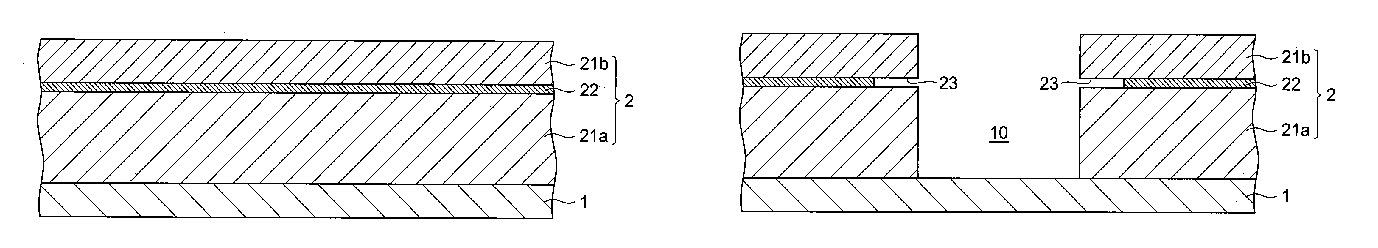
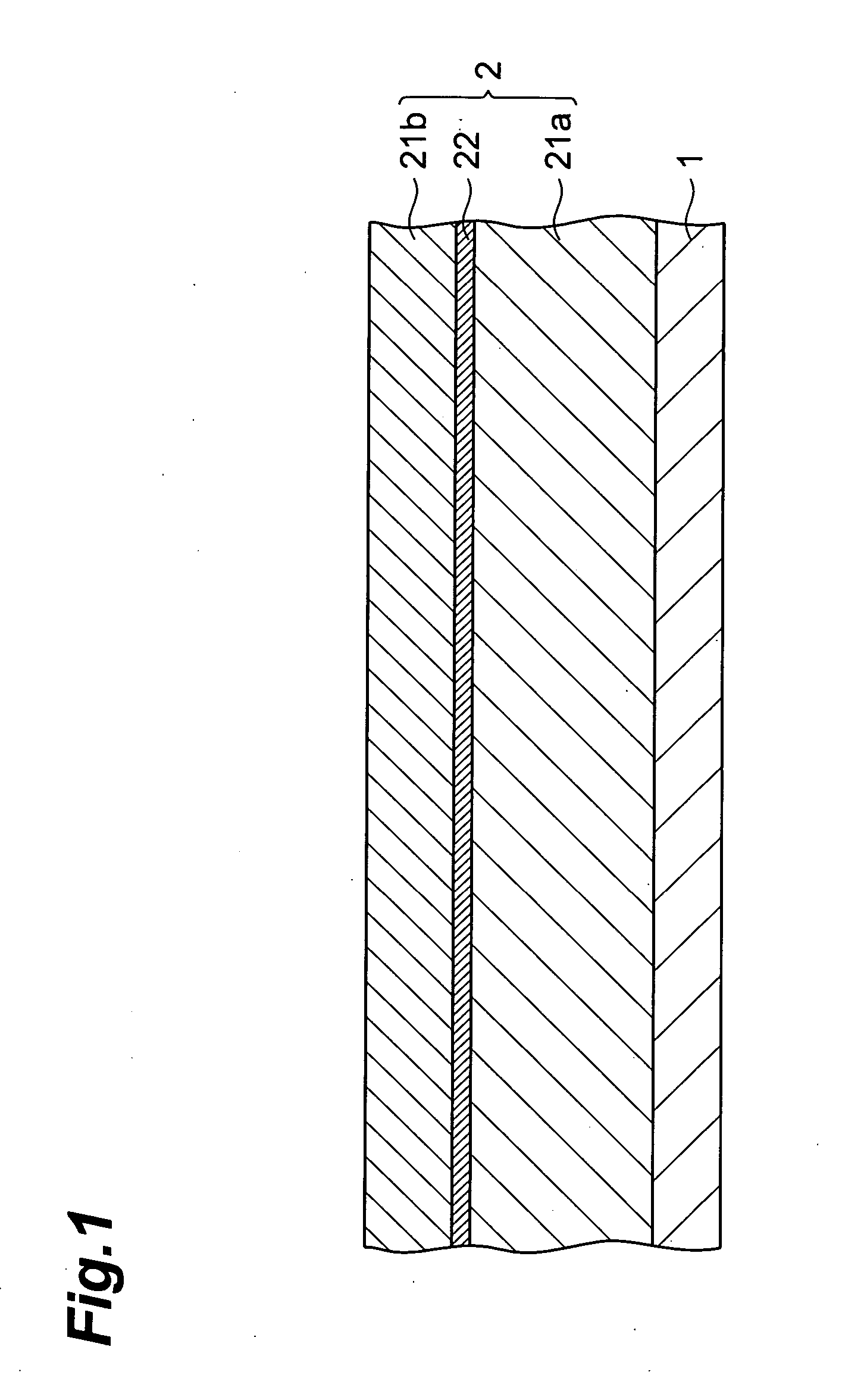
[0032]FIGS. 1, 2, 3, and 4 are sectional views for explaining the first embodiment of the method of forming a patterned material layer in accordance with the present invention.

[0033] In the first embodiment, as shown in FIG. 1, a resist layer 2 having a three-layer structure in which a first photosensitive resin layer 21a, an intermediate resin layer 22 soluble in a developing solution after being exposed to light, and a second photosensitive resin layer 21b are laminated in this order is initially formed on a substrate 1 (resist layer forming step).

[0034] The material for the substrate 1 is appropriately chosen according to the use of the material layer formed and the like. Specifically, substrates made of Si, ceramics (Al2O3.TiC, etc.), polymer materials, and the like are used.

[0035] The first photosensitive resin layer 21a and second photosensitive resin layer 21b are formed by spin coating or the like using a photosensitive resin which becomes soluble in a developing solution...

second embodiment

[0045]FIGS. 5, 6, 7, 8, and 9 are sectional views for explaining a second embodiment of the method of forming a patterned material layer in accordance with the present invention.

[0046] First, a resist layer 2 is formed on a substrate 1 (FIG. 5) in the second embodiment as well. The substrate 1 is one in which a plating electrode film 12 is formed on a support 11. The support 11 is the same as the substrate 1 in the first embodiment. The plating electrode film 12 is formed when a material which can be used as a plating electrode (which is preferably the same material as that of a plating layer 4 to be formed later) such as conductive metal, ceramics, or organic matter is formed into a film by a method such as sputtering, CVD, vapor deposition, or electroless plating. Then, the resist layer 2 having the same three-layer structure as that of the first embodiment is formed on the plating electrode film 12.

[0047] Subsequently, by way of the same exposing step and developing step as tho...

third embodiment

[0050]FIGS. 11 and 12 are sectional views for explaining a third embodiment of the method of forming a patterned material layer in accordance with the present invention.

[0051]FIG. 11 is a sectional view showing a state after the vacuum coating step, where the vacuum coating layer 3 is formed. In the third embodiment, side faces of the first photosensitive resin layer 21a are tilted in the resist pattern (resist layer 2) formed with a trench. This can incline the side faces of the material layer made of the plating layer 4 and material pattern part 31 with respect to a main surface of the substrate 1. The side faces of the first photosensitive resin layer 21a can be tilted, for example, when the first photosensitive resin layer 21a cured upon exposure to light is heated to its glass transition temperature or higher so as to be fluidized. Employing a photosensitive resin less transparent to exposure light as the first photosensitive resin 21a can also tilt the side faces of the first...


PUM


Abstract

A method of forming a patterned material layer, the method comprising: a resist layer forming step of forming a resist layer on a substrate, the resist layer including a first photosensitive resin layer, an intermediate resin layer, and a second photosensitive resin layer; an exposing step; a developing step of partly removing the resist layer so as to form a trench exposing the substrate and partly removing the intermediate resin layer so as to form a groove on a side face of the trench, thereby forming a resist frame; a vacuum coating step of forming a vacuum coating layer having a material pattern part covering the exposed part of the substrate and a part to lift off covering the resist frame; and a liftoff step of removing the part to lift off in the vacuum coating layer together with the resist frame, so as to yield a patterned material layer.

Description

BACKGROUND OF THE INVENTION [0001] 1. Field of the Invention [0002] The present invention relates to a patterned material layer, a method of forming the same, a microdevice, and a method of manufacturing the same. [0003] 2. Related Background Art [0004] In the manufacture of microdevices such as thin-film magnetic heads, thin-film inductors, semiconductor devices, thin-film sensors, and thin-film actuators, patterned material layers made of predetermined materials such as magnetic materials and conductive materials are formed by such methods as vacuum coating methods like sputtering and frame plating methods using resist frames (Japanese Patent Application Laid-Open Nos. HEI 11-175915, 2001-23984, and 2002-197612). SUMMARY OF THE INVENTION [0005] Methods forming a material layer by vacuum coating can easily turn various materials into thin films and can employ a wide range of materials. In the case of magnetic materials, for example, these methods are also advantageous in that they ...

Claims


Application Information

Patent Timeline
IPC IPC(8): H01L21/44
CPCG11B5/1278H01L21/76885H01L21/0272G11B5/3163Y10S438/951
Inventor KAMIJIMA, AKIFUMI
Owner TDK CORPARATION
Why Eureka
Try Eureka