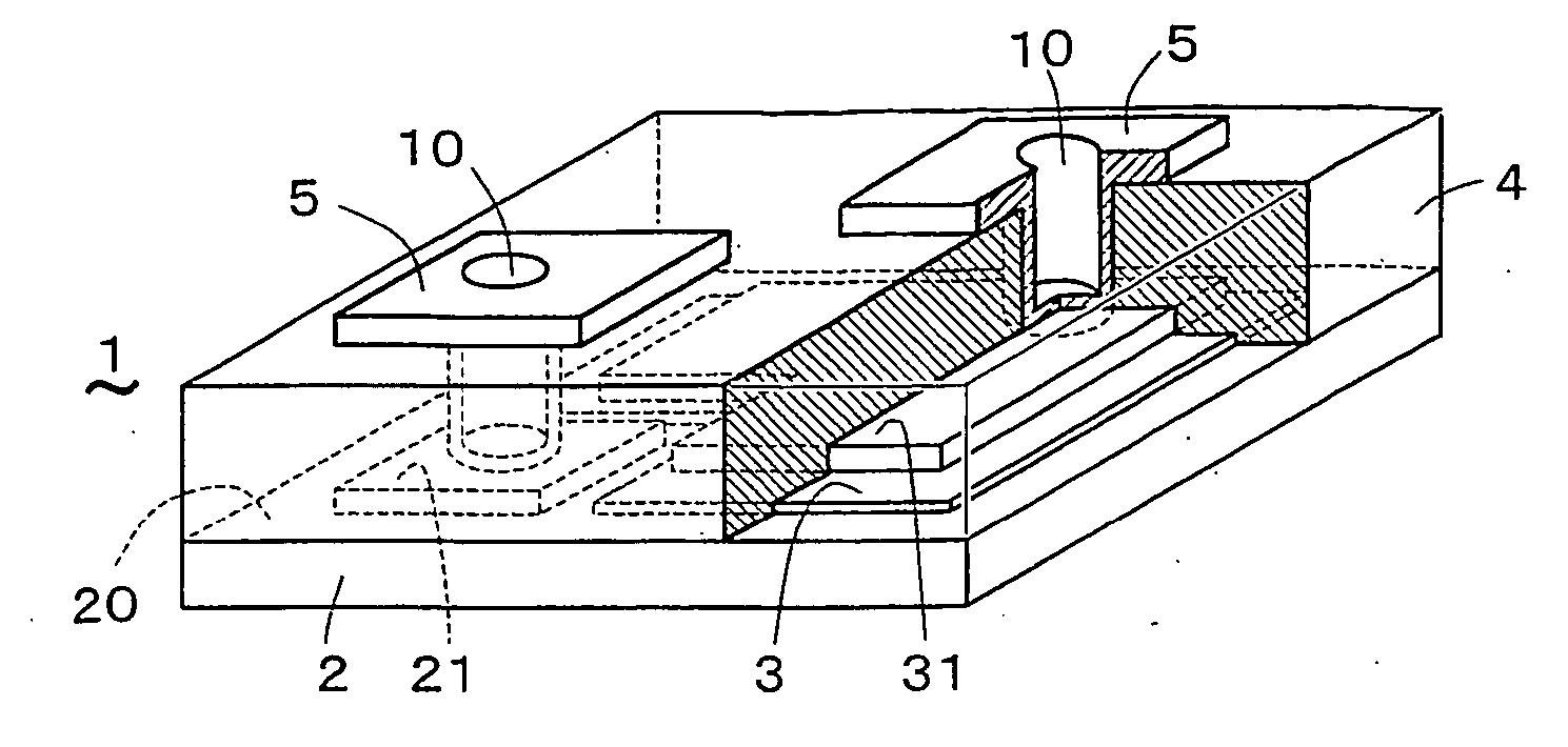
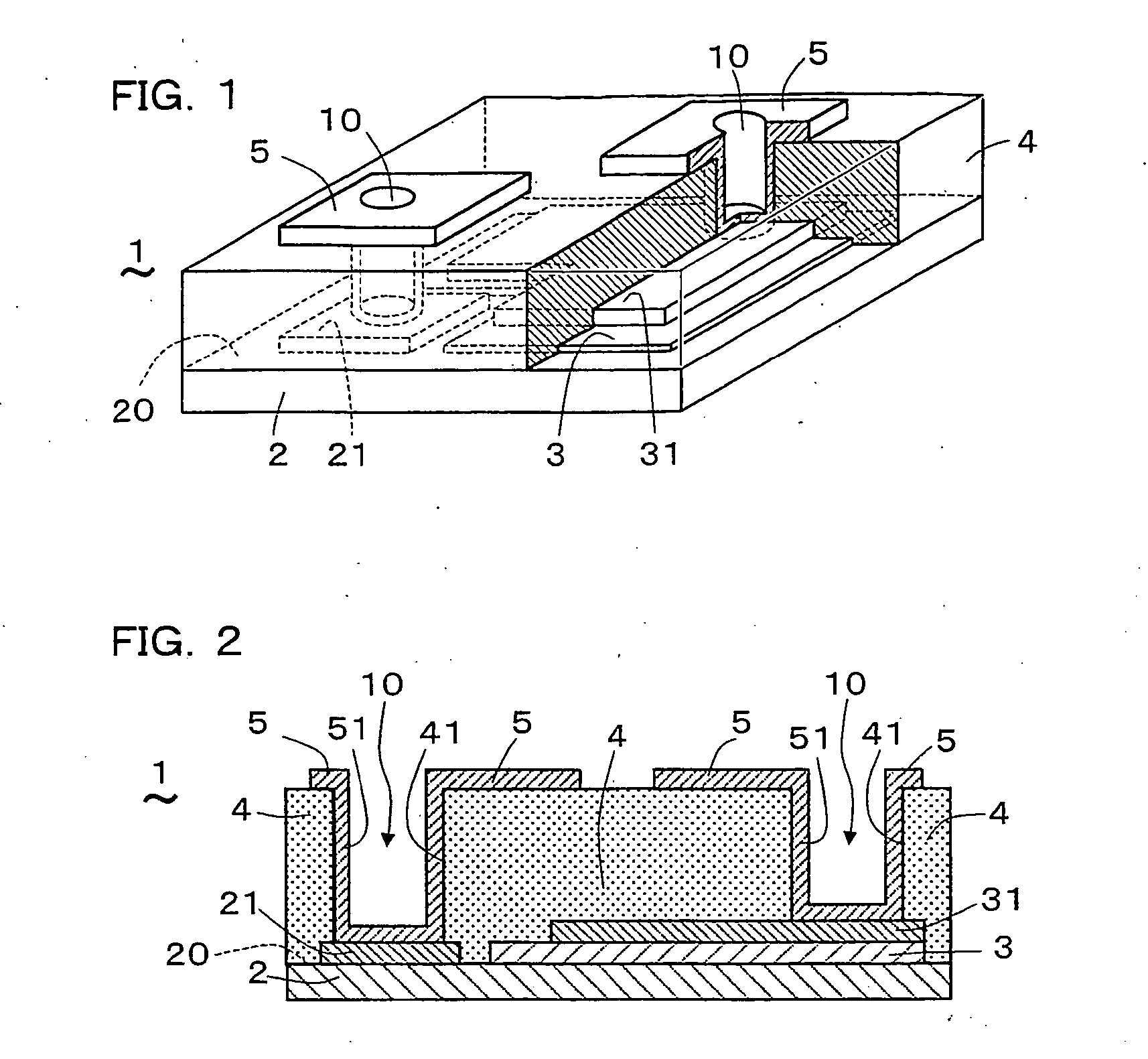
Semiconductor light-emitting device and its manufacturing method
- Summary
- Abstract
- Description
- Claims
- Application Information
AI Technical Summary
Benefits of technology
Problems solved by technology
Method used
Image

Examples
example 2
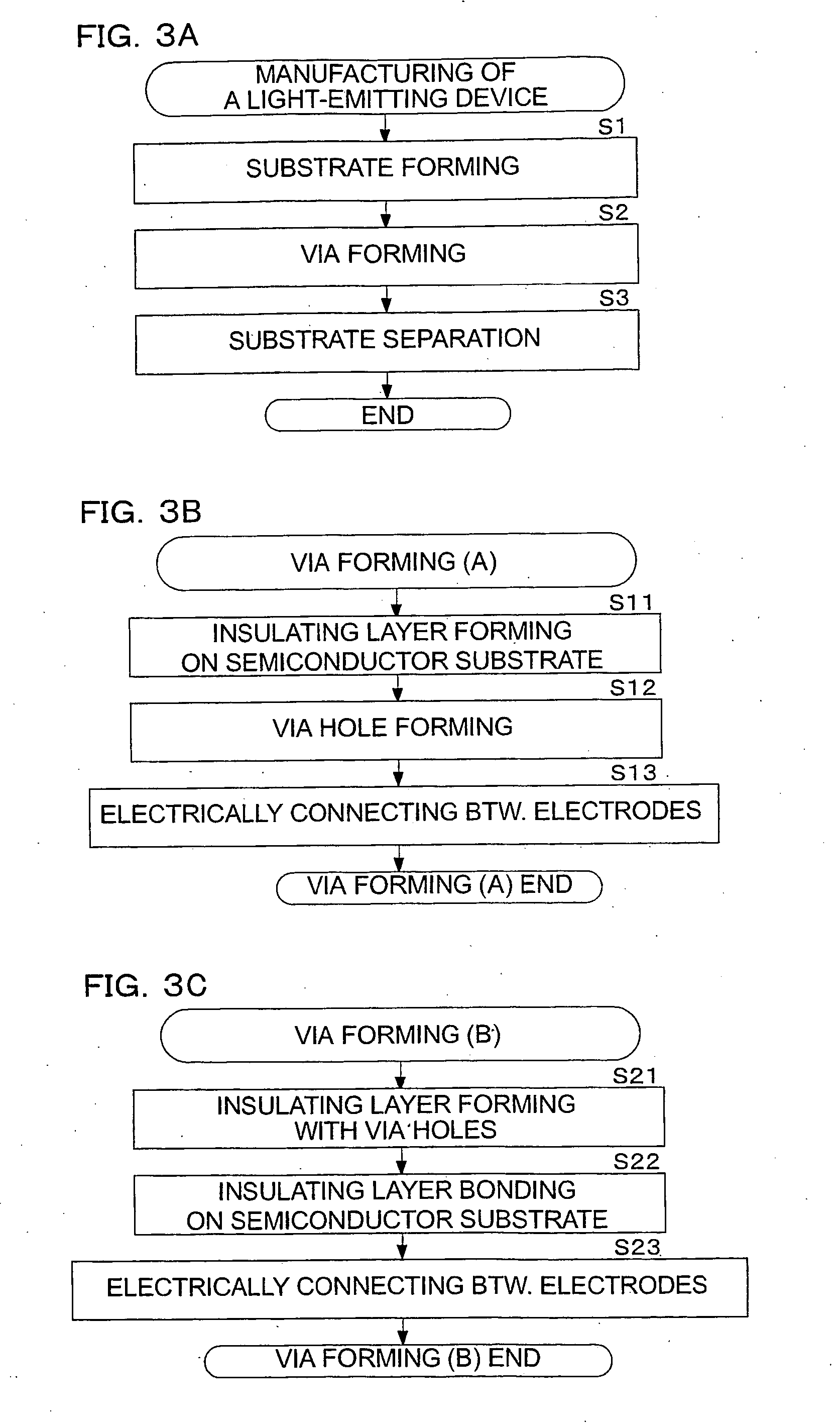
[0122] (Example 2 of Light-Emitting Device Manufacturing)
[0123] Another manufacturing method of the light-emitting device 1 is described with reference to FIG. 17A-17D. This manufacturing method uses the VIA forming process (B) shown in FIG. 3C. As shown in FIG. 17A, the insulating layer 4, in which VIA holes 41 corresponding to the semiconductor-surface-electrodes 21, 31 are pre-formed, is laminated and bonded to semiconductor layers 2, 3 and also semiconductor-surface-electrodes 21, 31 of the semiconductor-substrate.
[0124] As the material of insulating layer 4 for bonding use, resin, resin coated copper, ceramics for example alumina, and silicon can be used. The method to make VIA holes 41 in the insulating layer made of those material is practically the same as mentioned above, and the method using laser beams can be applied. In the case of silicon, VIA holes 41 can be made by plasma etching. In the case of ceramics, the ceramic insulating layer 4 may be prepared by firing of th...
example 3
[0126] (Example 3 of Light-Emitting Device Manufacturing)
[0127] Other manufacturing method of the light-emitting device 1 is described with reference to FIG. 18A, FIG. 18B, and FIG. 18C. In this manufacturing method, in the same manner mentioned above with reference to FIG. 7A, VIA holes 41 are pre-formed in the insulating layer 4, and moreover, the mount-surface-electrodes 5 and the electrical conductor 51 in the VIA holes 41 are also pre-formed in the insulating layer 4. Furthermore, VIA electrodes 52 which are corresponding to the semiconductor-surface-electrodes 21, 31 are also formed around VIA holes 41 on the surface of the insulating layer 4. Such VIA electrodes 52 are formed electrically and reliably to connect electrical conductor 51 and semiconductor-surface-electrodes 21, 31. In this method, the insulating layer 4 before bonding already has VIA's 10 and mount-surface-electrodes 5, in their final states.
[0128] By using such a insulating layer 4 having VIA's 10 and mount-s...
PUM
 Abstract
Description
Claims
Application Information
 - R&D Engineer
- R&D Manager
- IP Professional
- Industry Leading Data Capabilities
- Powerful AI technology
- Patent DNA Extraction
Browse by: Latest US Patents, China's latest patents, Technical Efficacy Thesaurus, Application Domain, Technology Topic.
© 2024 PatSnap. All rights reserved.Legal|Privacy policy|Modern Slavery Act Transparency Statement|Sitemap