
Electromechanical three-trace junction devices

a three-trace junction, electromechanical technology, applied in nanoelectromechanical switches, semiconductor/solid-state device details, instruments, etc., can solve the problems of low relative speed, power consumption, and long (millisecond) write cycles

Inactive Publication Date: 2006-10-19
NANTERO
View PDF29 Cites 48 Cited by
  • Summary
  • Abstract
  • Description
  • Claims
  • Application Information

AI Technical Summary

Problems solved by technology

ROM is relatively low cost but cannot be rewritten.
EEPROM (or “Flash”) is inexpensive, and has low power consumption but has long (millisecond) write cycles and low relative speed in comparison to DRAM or SRAM.
Flash also has a finite number of read / write cycles leading to low long-term reliability.
DRAM stores charges on transistor gates that act as capacitors, but its need to be electrically refreshed every few milliseconds complicates system design by requiring separate circuitry to “refresh” the memory contents before the capacitors discharge.
SRAM does not need to be refreshed and is fast relative to DRAM, but has lower density and is more expensive relative to DRAM.
Both SRAM and DRAM are volatile, meaning that if power to the memory is interrupted the memory will lose the information stored in the memory cells.
As the discussion above indicates, conventional memory solutions fail to possess all the desired characteristics.
Existing technologies that are nonvolatile are not randomly accessible and have low density, high cost, and limited ability to allow multiple writes with high reliability of circuit function.
Meanwhile, existing technologies that are volatile complicate system design or have low density.
However, both of these types of memory cells have relatively high resistance and low density.
A different MRAM memory cell based upon magnetic tunnel junctions has also been examined but has not led to large-scale commercialized devices.
However, FRAM suffers from a large memory cell size, and material incompatibility with standard semiconductor CMOS fabrication processes that make it difficult to manufacture large-scale integrated components.
Nonetheless, while the nonvolatility condition is met, this technology appears to suffer from slow operations, difficulty of manufacture and reliability problems, and has not reached a state of commercialization.
This form of memory requires highly specialized wire junctions and may not retain nonvolatility owing to the inherent instability found in redox processes.
These techniques are now believed to be difficult to employ at commercial scales using modem technology.
Moreover, they may contain inherent limitations such as the length of the nanotubes that may be grown reliably using these techniques, and it may be difficult to control the statistical variance of geometries of nanotube wires so grown.

Method used


Image

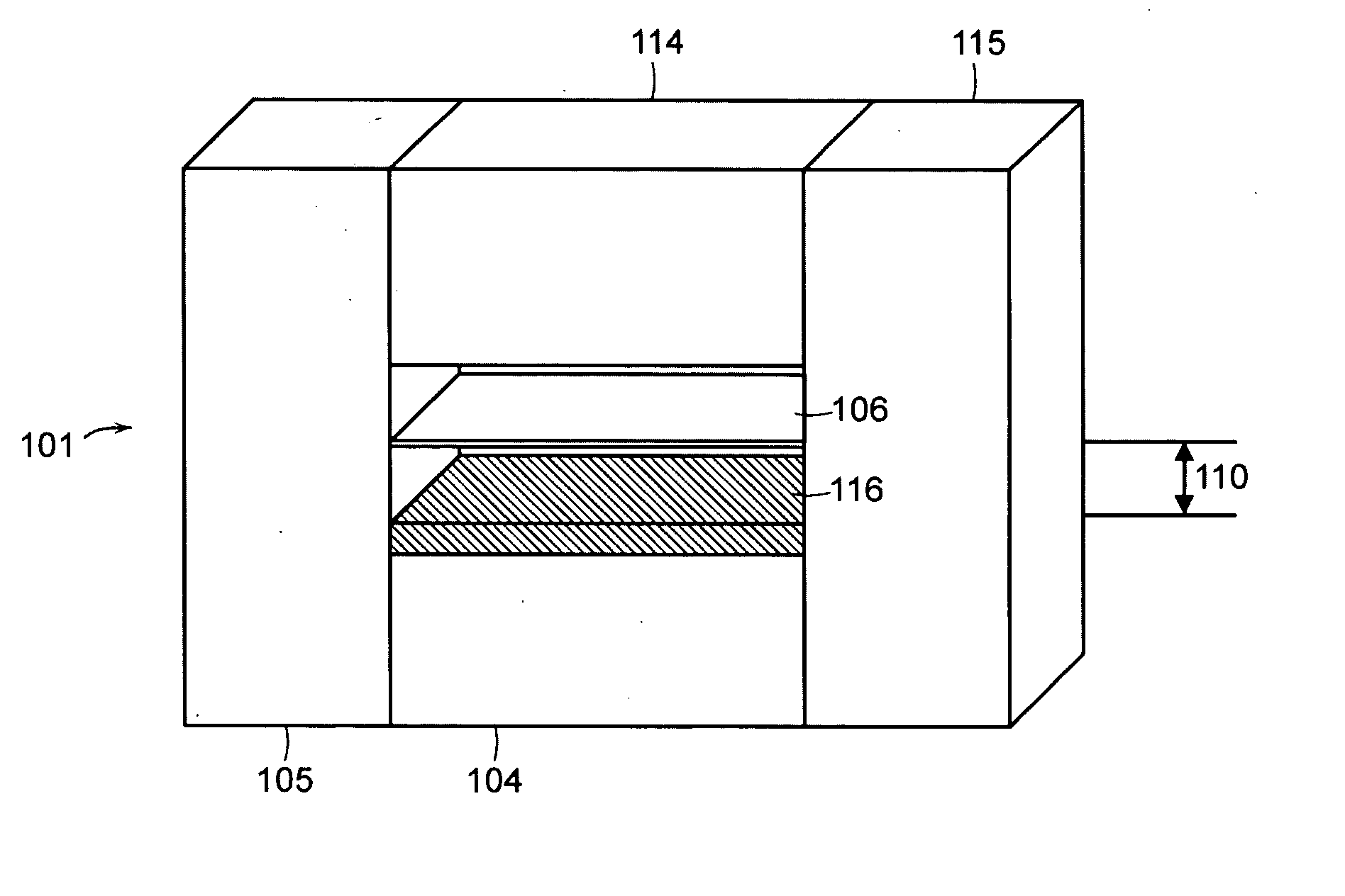
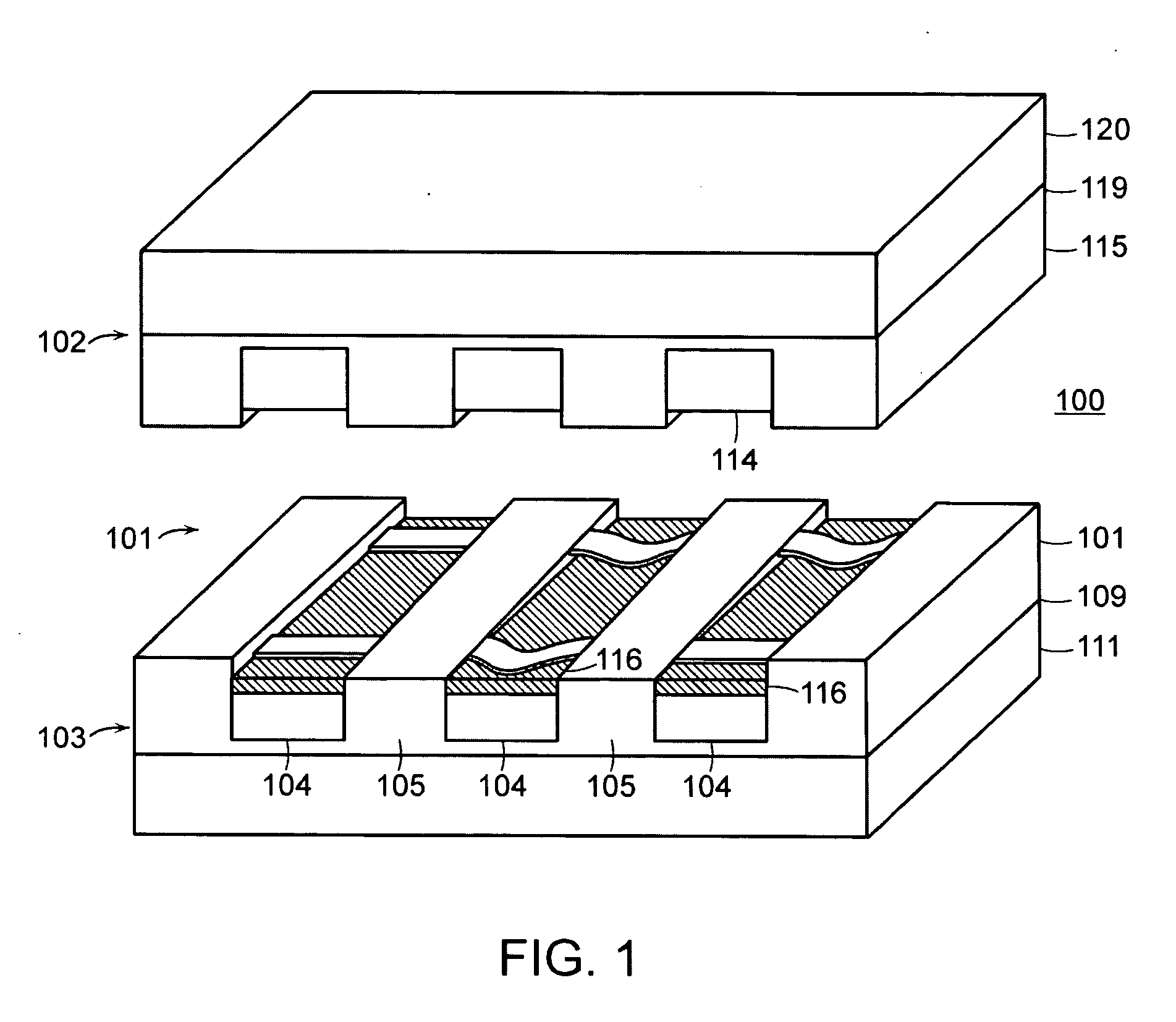
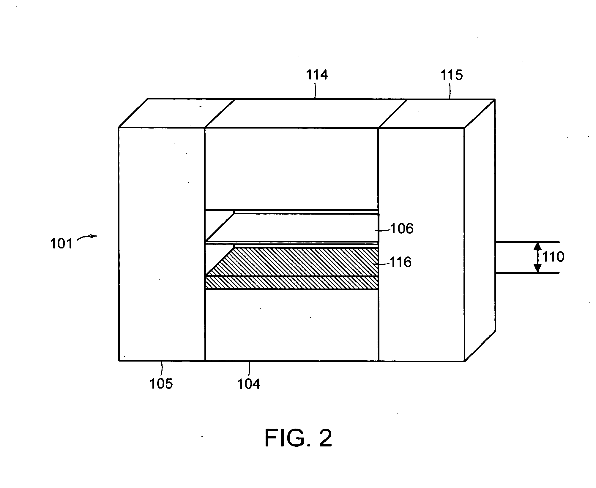
  • Electromechanical three-trace junction devices
  • Electromechanical three-trace junction devices
  • Electromechanical three-trace junction devices

Examples


example 1

[0091] A junction with metallic traces 510 was created as described in FIG. 5 and was oxidized as follows:

[0092] Five standard cubic centimeters per minute (sccm) of O2 was flowed over an NRAM switch, ac voltage (triangle wave) was applied to the NRAM junction (5 V amplitude, 10 kHz frequency).

[0093] Amplitudes lower than 2 V are not high enough to make the switch volatile. Amplitudes higher than 7 V frequently destroy the device (very high to infinite resistance afterwards). It was found that the switch turns volatile within a few seconds of application of voltage in the presence of the O2, after which, the switch remained volatile. 5V amplitude of ac wave adequately oxidizes the electrode; however voltage amplitudes of 2 V-7 V have been successfully used for fabricating volatile devices.

Additional Embodiments

[0094] In general, it should be noted that the feature sizes described above are suggested in view of modem manufacturing techniques. Other embodiments may be made with m...


PUM


Abstract

Three-trace electromechanical devices and methods of using same are described. The device of the present invention includes first and second electrically conductive elements with a nanotube ribbon (or other electromechanical elements) disposed therebetween. The nanotube ribbon is capable of maintaining its position after removing an electrical stimulus applied to at least one of the first and second electrically conductive elements. Such devices may be formed into arrays of cells. One of the conductive elements may be used to create an attractive force to cause the nanotube ribbon to contact a conductive element, and the other conductive element may be used to create an attractive force to pull the nanotube ribbon from contact with the contacted conductive element. The electrically conductive traces may be aligned or unaligned with one another.

Description

CROSS REFERENCE TO RELATED APPLICATIONS [0001] This application is a continuation of U.S. application Ser. No. 10 / 802,900, entitled “Electromechanical Tree-Trace Junction Devices,” filed Mar. 17, 2004, which is a continuation-in-part of U.S. application Ser. No. 10 / 033,323, entitled “Electromechanical Three-Trace Junction Devices,” filed Dec. 28, 2001. It is related to the following patent applications, all of which are incorporated by reference in their entirety: U.S. application Ser. No. 09 / 915,093, entitled “Electromechanical Memory Array Using Nanotube Ribbons and Method for Making Same,” filed Jul. 25, 2001; U.S. application Ser. No. 09 / 915,173 entitled “Electromechanical Memory Having Cell Selection Circuitry Constructed with Nanotube Technology,” filed Jul. 25, 2001; and U.S. application Ser. No. 09 / 915,095 entitled “Hybrid Circuit Having Nanotube Electromechanical Memory,” filed Jul. 25, 2001.BACKGROUND [0002] 1. Technical Field [0003] This invention relates in general to no...

Claims


Application Information

Patent Timeline
Patent Type & Authority Applications(United States)
IPC IPC(8): H01L27/10H01L29/73B81B3/00G11C11/56G11C13/02G11C23/00H01H1/00H01H59/00
CPCB82Y10/00G11C11/56G11C13/025G11C23/00Y10S977/943H01H1/0094Y10S977/742Y10S977/932Y10S977/936G11C2213/77
Inventor RUECKES, THOMASSEGAL, BRENT M.BERTIN, CLAUDE
Owner NANTERO
Learn More