Semiconductor device for high voltage IC

a high-voltage ic, semiconductor technology, applied in semiconductor devices, electronic switching, pulse techniques, etc., can solve the problems of affecting the operation of the device, the failure of the transistor, and the failure of the total circuit, so as to improve the switching speed of the device

Inactive Publication Date: 2006-10-19
DENSO CORP
View PDF4 Cites 11 Cited by
  • Summary
  • Abstract
  • Description
  • Claims
  • Application Information

AI Technical Summary

Benefits of technology

[0025] In the above device, a transmission passage provided by the second capacitor functions as a bypass passage of the input signal pulse for transmitting a potential of the pulse. Accordingly, when the input signal pulse starts to rise or when the input signal pulse starts to decay, the signal change is rapidly transmitted to each transistor through the bypass passage. Thus, the device has an additional pass

Problems solved by technology

Further, when each resistor has the same high resistance, the charge of the surge current is accommodated in the resistor, which is disposed far from the power source of the predetermined potential, so that the surge current cannot be discharged to the GND side.
Accordingly, a high voltage is applied to the transistor disposed far from the power source, so that the transistor may be b

Method used


Image

  • Semiconductor device for high voltage IC
  • Semiconductor device for high voltage IC
  • Semiconductor device for high voltage IC

Examples


first embodiment

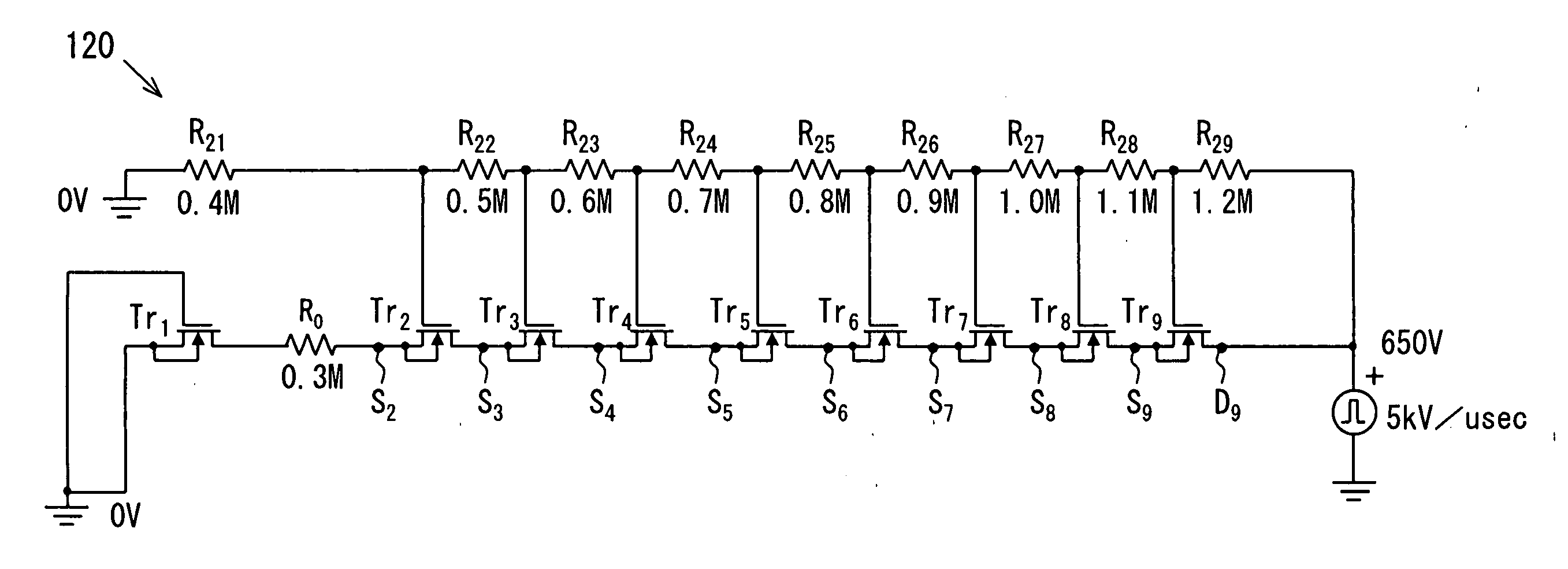
[0105] In view of the above points, a semiconductor device 120 of a first embodiment of the present invention is provided. FIG. 1 is an equivalent circuit diagram related to the semiconductor device 120 of a first embodiment.

[0106] The equivalent circuit diagram of the semiconductor device 120 shown in FIG. 1 owns a basically same arrangement with respect to the equivalent circuit diagram of the semiconductor device 100 shown in FIG. 24.

[0107] That is, in the semiconductor device 120 shown in FIG. 1, 9 pieces of transistor elements “Tr1” to “Tr9”, which are insulated / isolated from each other, are sequentially connected in a series connection manner between a ground (GND) potential of 0 V and a power supply potential of 650 V under such a condition that the GND-sided transistor element is defined as a first stage and the power supply-sided transistor element is defined as a ninth stage. 9 pieces of the transistor elements Tr1 to Tr9 of the semiconductor device 120 shown in FIG. 1 a...

second embodiment

[0122]FIG. 4 is an equivalent circuit diagram related to a semiconductor device 130 of a second embodiment of the present invention.

[0123] The equivalent circuit diagram of the semiconductor device 130 shown in FIG. 4 owns a basically different arrangement with respect to the equivalent circuit diagrams of the semiconductor devices 100 and 120 shown in FIG. 24 and FIG. 1.

[0124] That is, similar to the semiconductor devices 100 and 120 shown in FIG. 24 and FIG. 1, in the semiconductor device 130 shown in FIG. 4, 9 pieces of transistor elements “Tr1” to “Tr9”, which are insulated / isolated from each other, are sequentially connected in a series connection manner between a ground (GND) potential of 0 V and a power supply potential of 650 V under such a condition that the GND-sided transistor element is defined as a first stage and the power supply-sided transistor element is defined as a ninth stage. It should be understood that 9 pieces of the transistor elements Tr1 to Tr9 in the se...


PUM


Abstract

A semiconductor device includes: a plurality of transistors connected in series between a ground potential and a predetermined potential; an input terminal provided by a gate terminal of the first step transistor; a plurality of resistors connected in series between the ground potential and the predetermined potential; and an output terminal provided by a predetermined potential side terminal of the Nth step transistor. A gate terminal of each transistor other than the first step transistor is sequentially connected between neighboring two resistors. One of the resistors defined as an Ith step resistor has a resistance, which is smaller than a resistance of a (I+1)th step resistor.

Description

CROSS REFERENCE TO RELATED APPLICATIONS [0001] This application is based on Japanese Patent Applications No. 2005-121306 filed on Apr. 19, 2005, and No. 2005-318679 filed on Nov. 1, 2005, the disclosures of which are incorporated herein by reference. FIELD OF THE INVENTION [0002] The present invention relates to a semiconductor device for a high voltage IC. BACKGROUND OF THE INVENTION [0003] High voltage ICs for driving inverters and the like have been disclosed in, for instance, Japanese Patent No. 3384399 (which corresponds to U.S. Pat. No. 5,736,774), and Proceedings of ISPSD '04, pages 375-378, H. Akiyama et al. by Mitsubishi Electric Company. [0004]FIG. 22A is a circuit arrangement diagram for showing a power portion of a motor controlling inverter which is disclosed in U.S. Pat. No. 5,736,774. Power devices (namely, IGBTs Q1 to Q6, and diodes D1 to D6) employed so as to drive a three-phase motor Mo constitute a bridge circuit, and are constructed in the structure of a power mo...

Claims


Application Information

Patent Timeline
IPC IPC(8): H01L29/768
CPCH03K17/102H01L27/1203
Inventor YAMADA, AKIRAHIMI, HIROAKIAKAGI, NOZOMUNAGATA, JUNICHI
Owner DENSO CORP
Why Eureka
Try Eureka