Two-terminal solid-state memory device and two-terminal flexible memory device based on nanocrystals or nanoparticles

a technology of flexible memory and solid-state memory, which is applied in the field of memory devices, can solve the problems of limiting the dimensions of the device and thus the device density in the chip, and achieve the effects of less fabrication steps, improved chip density, and simplified design

Inactive Publication Date: 2006-10-19
NANYANG TECH UNIV
View PDF5 Cites 45 Cited by
  • Summary
  • Abstract
  • Description
  • Claims
  • Application Information

AI Technical Summary

Benefits of technology

[0006] The above object has been realized in a MOS structure with a high concentration of nanocrystals embedded throughout the gate oxide wherein the previous problems are eliminated. In contrast to the conventional situation in which charge trapping in nanocrystals confined in a narrow layer embedded in the gate oxide of MOSFETs leads to a shift in threshold voltage, charge trapping in nanocrystals distributing throughout the gate oxide of MOS devices in the present invention leads to modulations in capacitance, gate oxide resistance, and gate current. The modulated capacitance, gate oxide resistance, and gate current can be recovered after the release of the trapped charges. These modulations, especially the gate oxide resistance modulation, allow the device to behave as “on” or “off” state. And as such a memory structure has only two terminals, i.e., the gate and the substrate (here no source and drain terminals are required), it can be fabricated with a simpler design and less fabrication steps. Furthermore, the device density in a chip can be substantially increased because of the use of the two-terminal devices with elimination of source / drain areas.

Problems solved by technology

The resolution of photolithography will limit the dimensions of the device and thus the device density in the chip.

Method used


Image

  • Two-terminal solid-state memory device and two-terminal flexible memory device based on nanocrystals or nanoparticles
  • Two-terminal solid-state memory device and two-terminal flexible memory device based on nanocrystals or nanoparticles
  • Two-terminal solid-state memory device and two-terminal flexible memory device based on nanocrystals or nanoparticles

Examples


Embodiment Construction

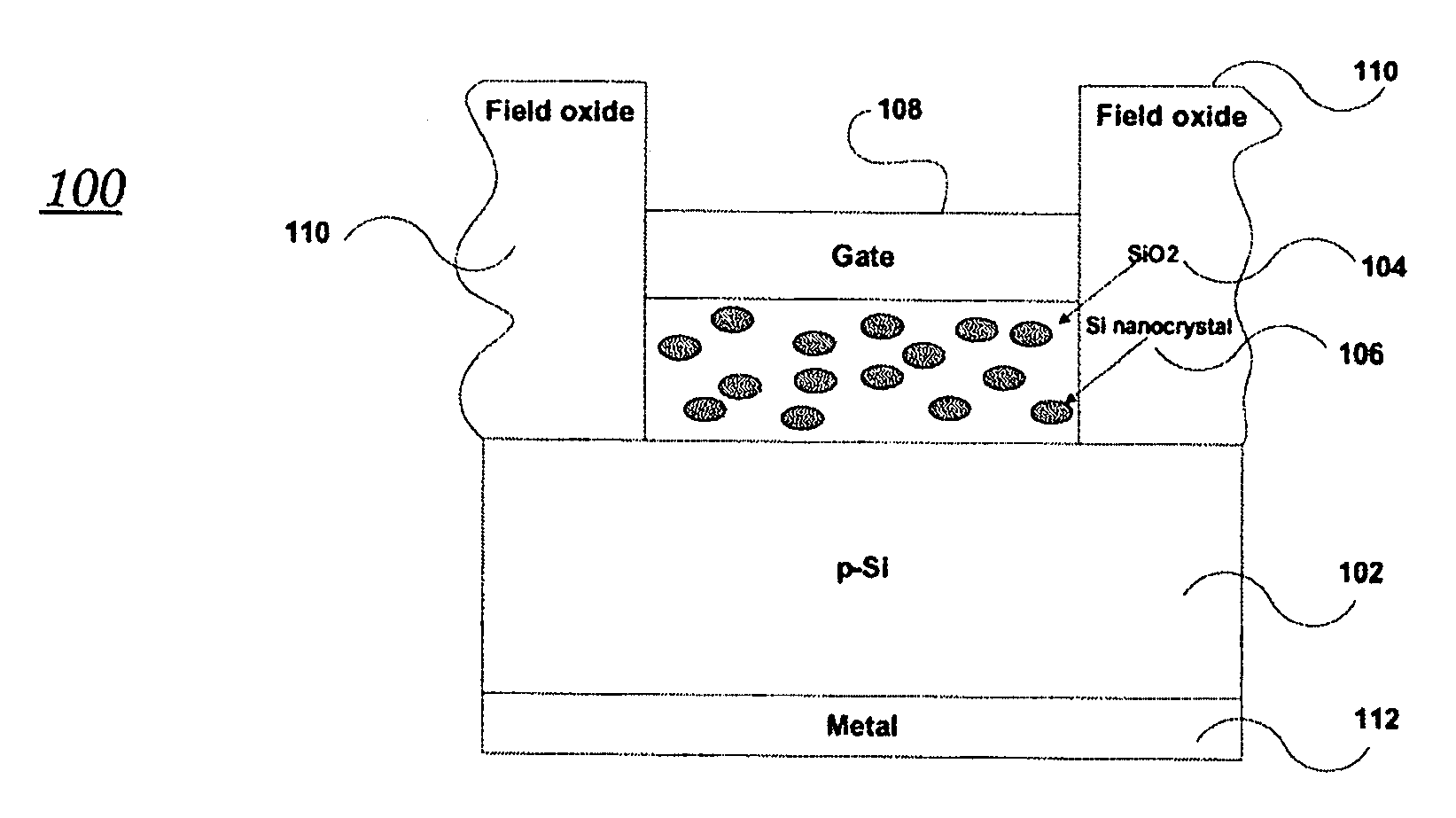
[0019]FIG. 1 is a cross section view of a two-terminal solid-state memory device 100 according to an embodiment of the present invention. In the illustrated embodiment, the device 100 includes a substrate 102, a dielectric layer 104 disposed on the substrate 102, several nanocrystals and / or nanoparticles 106 disposed in the dielectric layer 104, a gate electrode 108 disposed on the dielectric layer 104, and an insulating layer 110 disposed on the substrate 102. A metal electrode 112 may be disposed on the backside of the substrate 102 as the second terminal.

[0020] In embodiments of the present invention, the nanocrystals and / or nanoparticles 106 are distributed throughout the dielectric layer 104. In one embodiment, the peak concentration of nanocrystals and / or nanoparticles 106 may be located near the gate electrode 108.

[0021] In one embodiment, the substrate 102 may be a p-type semiconductor substrate, such as (100) silicon (Si), for example. In an alternative embodiment, the su...


PUM

PropertyMeasurementUnit
sizeaaaaaaaaaa
sizeaaaaaaaaaa
sizeaaaaaaaaaa

Abstract

A two-terminal memory device based on semiconductor (such as Si or Ge) or metal (such as Al or Au) nanocrystals and / or nanoparticles is described wherein each device has a substrate, a dielectric layer (such as SiO2 or organic dielectric materials) nanocrystals and / or nanoparticles distributed throughout the dielectric layer, and a metal (or poly-crystalline Si, or conductive organic materials) gate electrode. The memory states of the device are distinguished by charging and discharging the nanocrystals and / or nanoparticles. This two-terminal memory device is much simpler than the conventional four-terminal MOSFET-based memory device in terms of device structure and fabrication process. In addition, it is flexible if the memory devices are fabricated on flexible substrate with organic materials.

Description

BACKGROUND [0001] 1. Field [0002] Embodiments of the present invention relate to memory devices and in particular to two-terminal memory devices. [0003] 2. Discussion of Related Art [0004] In recent years, it is found that semiconductor nanocrystals are effective in storing electric charges, which has been proposed as a basis for the development of nonvolatile memory devices. Commonly used approach for fabricating such memory devices is based on conventional MOSFET processes. The resulting devices include a substrate with source and drain regions, a gate oxide above the substrate with nanocrystals (<10 nm) embedded in 2-3 nm close to the substrate. The advantage of this type of device is that nonvolatile memories can be formed, particularly devices of ultra-low power consumption, ultra-high density in the chip and with simpler design. Examples are described in U.S. Pat. No. 6,320,784 to Muralidhar et al. and U.S. Pat. No. 6,690,059 to Lojek. [0005] However, there are many times o...

Claims


Application Information

Patent Timeline
Patent Type & Authority Applications(United States)
IPC IPC(8): H01L29/792
CPCB82Y10/00G11C13/0014H01L29/51H01L21/28273H01L29/42332G11C2216/06H01L29/40114
Inventor CHEN, TUPEILIU, YANGNG, CHI YUNGTSE, MAN SIU
Owner NANYANG TECH UNIV
Why Eureka
Try Eureka