
Plasma display panel

a technology of plasma display panel and display panel, which is applied in the direction of conveyors, instruments, and electrodes, can solve the problems of increasing the manufacturing cost of the plasma display panel, and achieve the effects of increasing the aperture ratio, reducing the discharge initiation voltage level, and increasing the discharge diffusion efficiency

Inactive Publication Date: 2006-10-19
LG ELECTRONICS INC
View PDF5 Cites 8 Cited by
  • Summary
  • Abstract
  • Description
  • Claims
  • Application Information

AI Technical Summary

Benefits of technology

[0015] According to the embodiments of the present invention, the plasma display panel structure can increase an aperture ratio, reduce a discharge initiation voltage level and increase discharge diffusion efficiency within the discharge cell. On the basis of these advantages, transparent electrodes are not necessarily formed, thereby reducing plasma display panel manufacturing costs.

Problems solved by technology

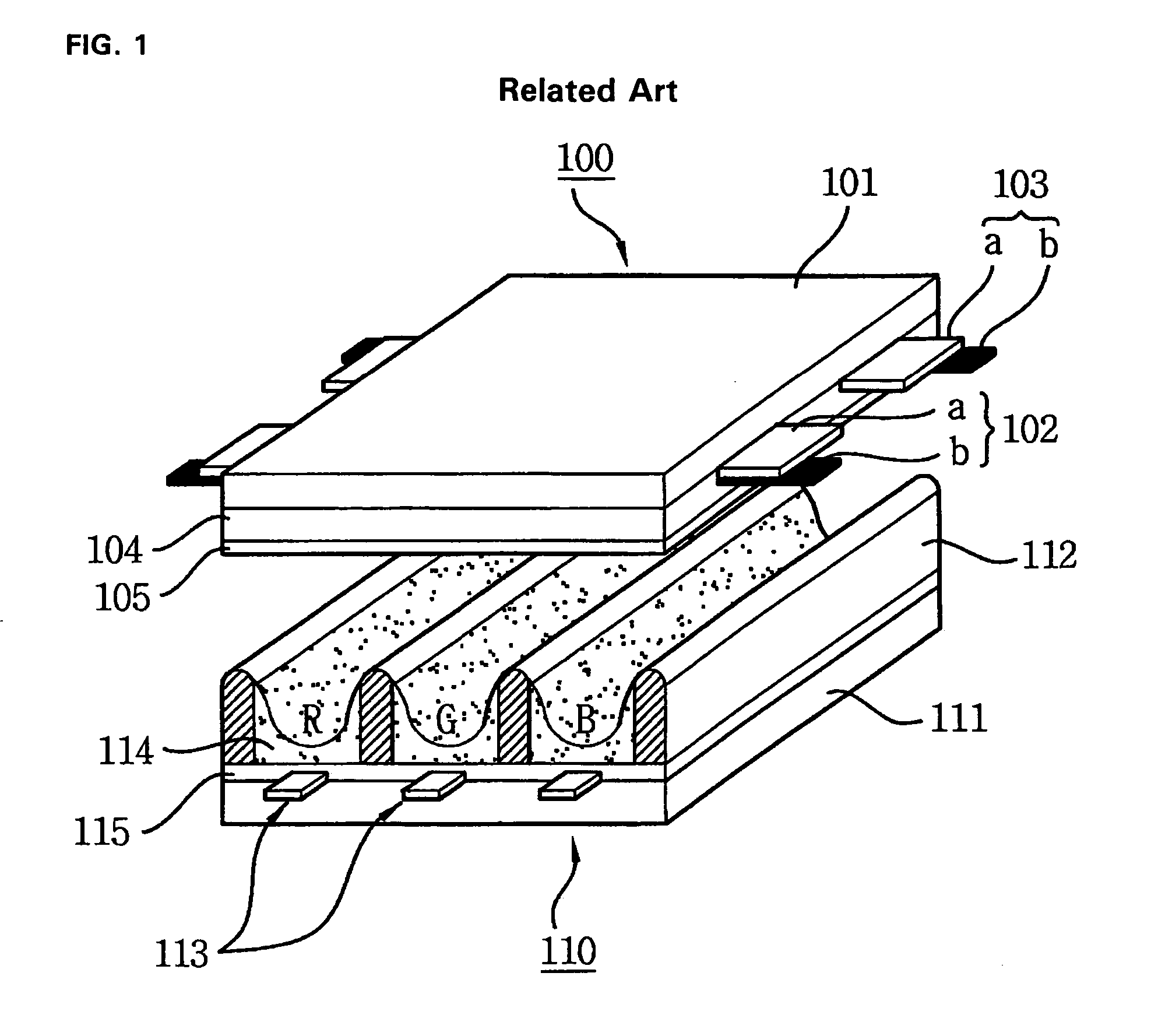
The transparent electrodes 102a and 103a become one cause for increasing manufacturing costs for the plasma display panel.

Method used


Image

  • Plasma display panel
  • Plasma display panel
  • Plasma display panel

Examples


first embodiment

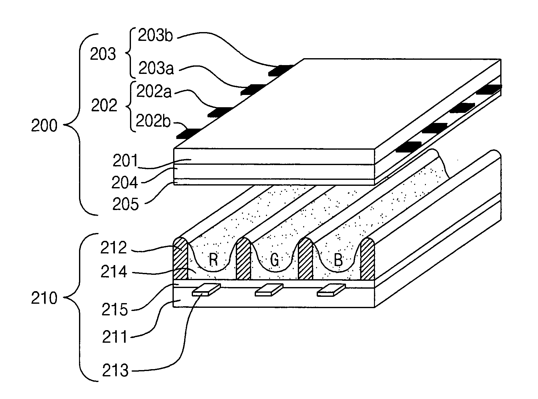
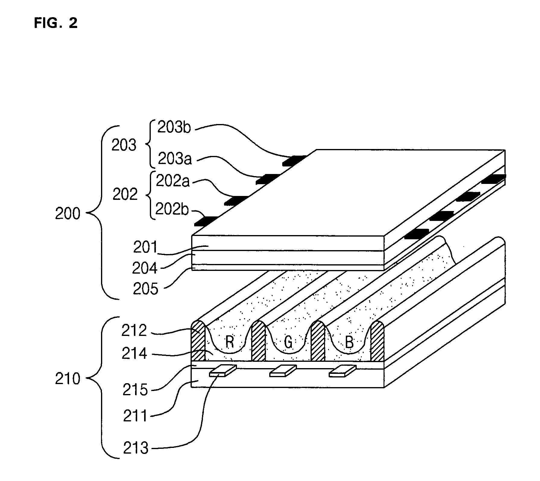
[0054]FIG. 2 illustrates a plasma display panel according to a first embodiment of the present invention.

[0055] As illustrated in FIG. 2, the plasma display panel according to the first embodiment of the present invention comprises a front panel 200 and a rear panel 210, which are connected to each other with a certain distance therebetween. Also, the plasma display panel comprises address electrodes 213, which are formed over a rear substrate 211 in the direction of intersecting a pair of sustain electrodes 202 and 203, and barrier ribs 212, which partition plurality of discharge cells and are formed between a front substrate 201 and the rear substrate 211.

[0056] The front panel 200 comprises the aforementioned pair of the sustain electrodes 202 and 203 arranged over the front substrate 201. The pair of the sustain electrodes 202 and 203 is classified into a scan electrode 202 and a sustain electrode 203 depending on functions thereof, a driving pulse of each of the scan electrod...

second embodiment

[0068]FIG. 4 illustrates a plasma display panel according to a second embodiment of the present invention.

[0069] As illustrated in FIG. 4, the plasma display panel according to the second embodiment of the present invention comprises a front panel 400 and a rear panel 410, which are connected to each other with a certain distance therebetween. Also, the plasma display panel comprises address electrodes 413, which are formed over a rear substrate 411 in the direction of intersecting a pair of the sustain electrodes 402 and 403, and barrier ribs 412, which partition plurality of discharge cells and, are formed between a front substrate 401 and the rear substrate 411. Herein, detailed description of those characteristics of the plasma display panel according to the second embodiment, which are substantially identical to those of the plasma display panel according to the first embodiment, will be omitted.

[0070] The pair of the sustain electrodes 402 and 403 are formed of opaque metal ...


PUM


Abstract

A plasma display panel is provided. Particularly, an embodiment of the present invention suggests a sustain electrode structure comprising opaque electrodes instead of transparent electrodes to improve an aperture ratio. The number of electrode lines pertained to each sustain electrode is suggested to improve the aperture ratio, and a first projection electrode projecting to a central portion of a discharge cell from the electrode line can allows a discharge initiation voltage level to be decreased. A second projection electrode projecting in a direction away from the central portion of the discharge cell can be advantageous of increasing discharge diffusion efficiency within the discharge cell.

Description

[0001] This non-provisional application claims priority under 35 U.S.C. § 119(a) on Patent Application No. 10-2005-0026756 filed in Korea on Mar. 30, 2005 the entire contents of which are hereby incorporated by reference. BACKGROUND OF THE INVENTION [0002] 1. Field of the Invention [0003] The present invention relates to a display apparatus, and more particularly, to a plasma display panel. [0004] 2. Description of the Related Art [0005] In a typical plasma display panel, a barrier rib formed between a front substrate and a rear substrate composes one unit cell. Each of the unit cells is filled with a main discharge gas such as neon (Ne), helium (He) or a mixture gas of Ne and He and an inert gas containing a trace amount of xenon. When a discharge event occurs by a high voltage frequency, the inert gas generates vacuum ultraviolet rays and causes phosphors formed between the barrier ribs to emit light to thereby realize an image. Such a plasma display panel can be configured to be ...

Claims


Application Information

Patent Timeline
IPC IPC(8): H01J17/49G09G3/28H01J11/12H01J11/22H01J11/24H01J11/26H01J11/28H01J11/34H01J11/36H01J11/38H01J11/40H01J11/42H01J11/44H01J11/50
CPCH01J11/12H01J2211/323H01J2211/245H01J11/24B65B43/42B65B57/04B65G43/08B65G47/8823B65G2201/0238
Inventor KIM, WOOTAE
Owner LG ELECTRONICS INC
Learn More