Multi-power source semiconductor device
a technology of power source semiconductors and semiconductor devices, applied in the direction of generating/distributing signals, pulse techniques, instruments, etc., can solve the problems of delay circuits that may increase the amount of delay, and achieve the effect of reducing clock skew
- Summary
- Abstract
- Description
- Claims
- Application Information
AI Technical Summary
Benefits of technology
Problems solved by technology
Method used
Image
Examples
first embodiment
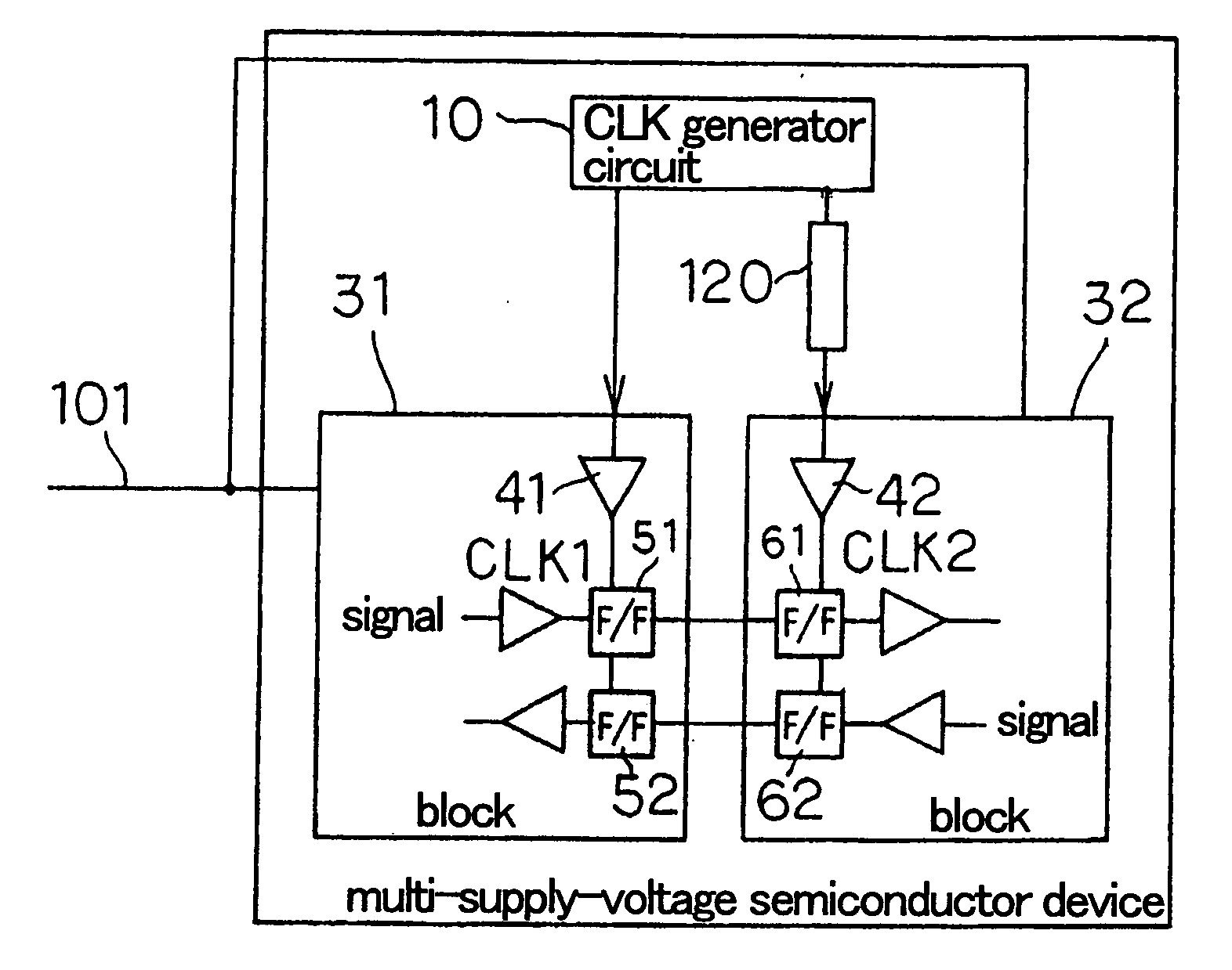
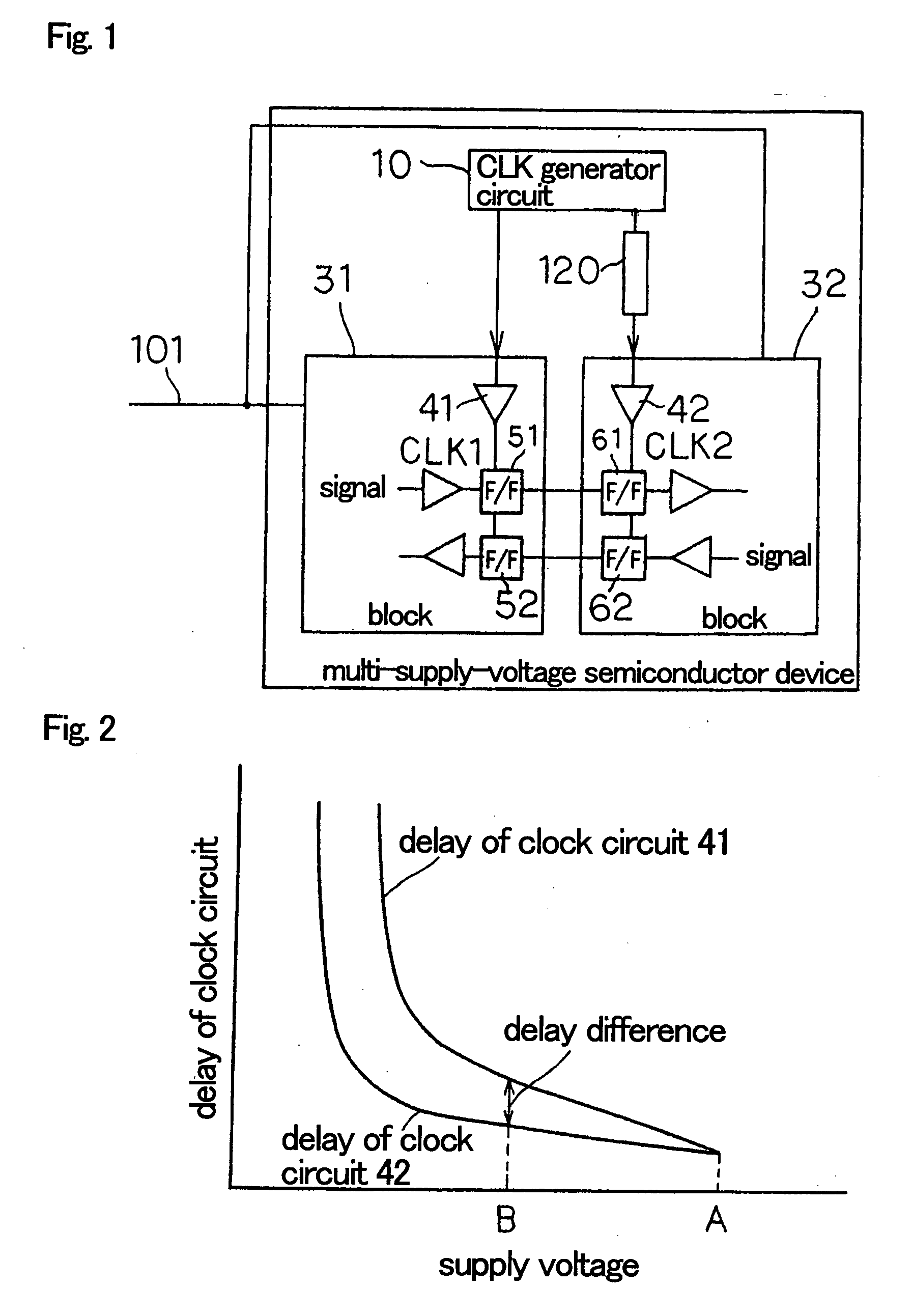
[0101]FIG. 6 is a block diagram showing a configuration of a multi-supply-voltage semiconductor device according to a first embodiment of the present invention. Components in FIG. 6 that are the same as those in FIG. 1 are labeled the same reference numerals, the description of which will be omitted.
[0102] A multi-supply-voltage semiconductor device according to the first embodiment includes clock (CLK) generator circuit 10, blocks 31, 32, and variable delay circuit 20. The multi-supply-voltage semiconductor device of the first embodiment has a configuration in which delay circuit 120 of the multi-supply-voltage semiconductor device shown in FIG. 1 is replaced with variable delay circuit 20.
[0103] Inputted into the multi-supply-voltage semiconductor device of the first embodiment is variable power supply 101 the power supply voltage of which changes. Variable power supply 101 is supplied to variable delay circuit 20 as well as to blocks 31, 32. If variable power supply 101 is the ...
second embodiment
[0119] A multi-supply-voltage semiconductor device according to a second embodiment of the present invention will be described below. FIG. 12 is a block diagram showing a configuration of a multi-supply-voltage semiconductor device according to the second embodiment of the present invention. Components in FIG. 12 that are the same as those in FIG. 6 are labeled the same reference numerals, the description of which will be omitted.
[0120] While the multi-supply-voltage semiconductor device in the first embodiment of the present invention descried above has a variable delay circuit provided in one of its blocks, the multi-supply-voltage semiconductor device in the second embodiment of the present invention has variable delay circuits provided in multiple or in all blocks as shown in FIG. 12.
[0121] If clock circuit 41 is formed by high-threshold transistors and clock circuit 42 is formed by low-threshold transistors, variable delay circuit 20 will be formed by high-threshold transisto...
third embodiment
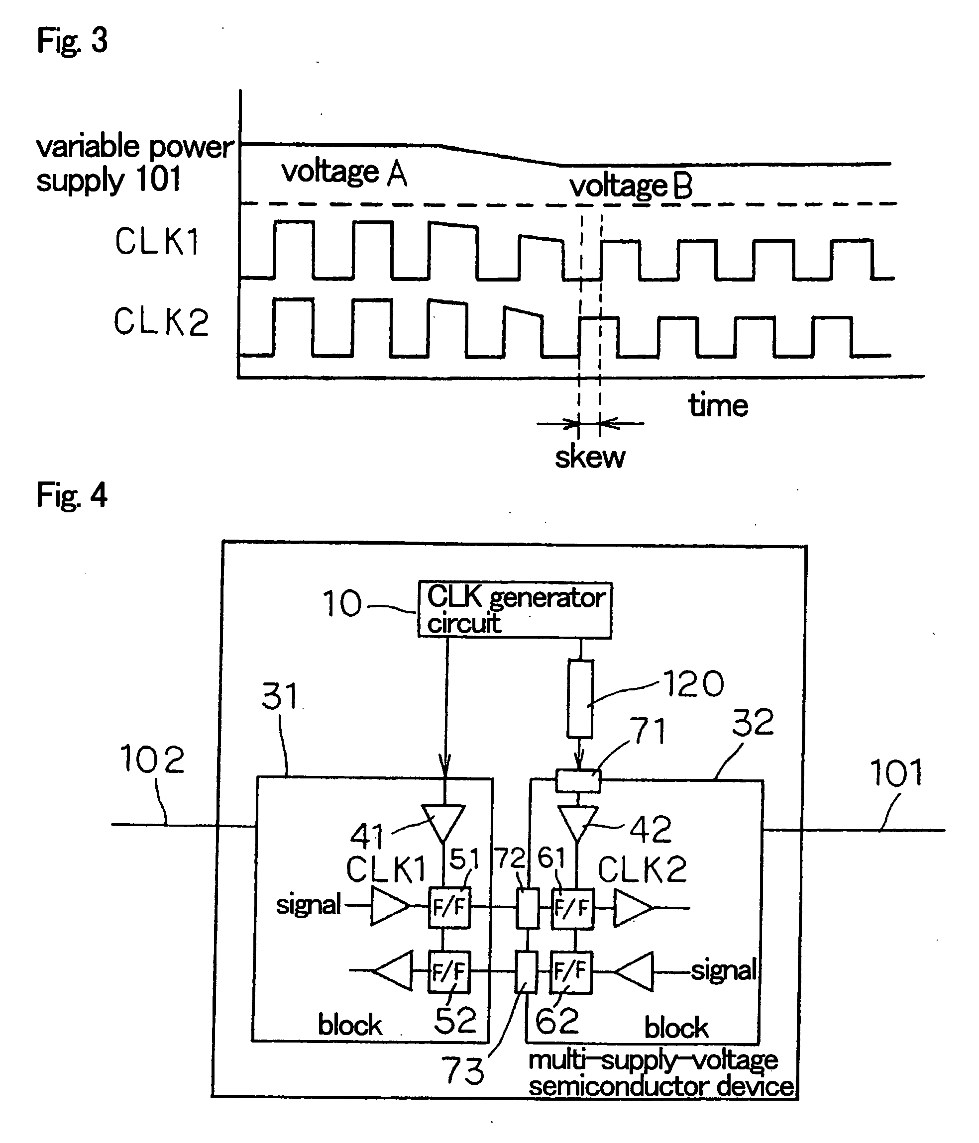
[0124] A multi-supply-voltage semiconductor device according to a third embodiment of the present invention will be described below. In the first and second embodiments described above, variable delay circuit 20 is provided to reduce clock skew due to a change in voltage of variable power supply 101 to stabilize operation of the blocks. However, a malfunction can occur if changes in delays of variable delay circuit 20 and clock circuits 41, 42 go out of synchronization while the voltage of variable power supply 101 is changing. The multi-supply-voltage semiconductor device of the third embodiment stops a clock signal supplied from clock generator circuit 10 during a change in the power supply voltage in order to stabilize operation of the blocks.
[0125] The multi-supply-voltage semiconductor device of the third embodiment further includes voltage change detector circuit 90 and AND circuits 91, 92, as shown in FIG. 13, in addition to the components of the multi-supply-voltage semicon...
PUM
 Abstract
Description
Claims
Application Information


