Method for improving efficiency in laying out electronic components

a technology of electronic components and efficiency, applied in the field of electronic component efficiency improvement, can solve the problems of time-consuming and labor-intensive electronic component fabrication, before electronic product fabrication, placement errors, etc., and achieve the effect of improving efficiency in electronic component fabrication, improving efficiency in electronic component assembly, and shortening research tim

Inactive Publication Date: 2006-10-19
INVENTEC CORP
View PDF6 Cites 0 Cited by
  • Summary
  • Abstract
  • Description
  • Claims
  • Application Information

AI Technical Summary

Benefits of technology

[0008] In light of the above prior-art drawbacks, an objective of the present invention is to provide a method for improving efficiency in laying out electronic components, whereby the electronic components contained in a circuit diagram can be rapidly and precisely placed in a printed circuit board.
[0009] Another objective of the present invention is to provide a method for improving efficiency in laying out electronic components, so that subsequent placement of the electronic components in a printed circuit board no longer requires modifications to electronic circuits, so as to effectively shorten the research time.
[0010] In accordance with the above and other objectives, the present invention proposes a method for improving efficiency in laying out electronic components, applicable to the layout operation for the electronic components of a printed circuit board. Initially, a first two-dimensional planar view containing the various electronic components numbers therein is preset using a drafting software platform. Subsequently, the two-dimensional planar view is converted into a text file and all the data contained in the two-dimensional planar view are recorded in the text file. Then, all of the electronic component numbers contained in the first two-dimensional planar view are displayed in a second two-dimensional planar view, and a function selection menu is generated by an arithmetic process, such that a user can select electronic component numbers contained in the text file to perform placement of the electronic components.
[0011] Using the method proposed in the present invention, the placement of the electronic components can be rapidly and precisely performed by an electronic engineer and a layout engineer so as to increase layout speed for electronic components and accelerate the design process. Furthermore, when the electronic engineer decides to modify the circuit or replace an electronic component, according to the method proposed in the present invention, the desired electronic component to be modified or replaced can be immediately located, so as to simplify the procedure required for changing electronic component layout.

Problems solved by technology

However, a fabrication of printed circuit boards (PCBs) for the electronic products, which fabrication involves designing, circuit drafting, mechanical drafting, component placement, and drafting of a layout diagram for the printed circuit board, before fabrication of electronic products, is time-consuming.
Such searching, in order to place the electronic components one-by-one into the printed circuit board layout, can be very time-consuming and placement errors can occur.
Moreover, as the variety of electronic components has gradually increased and components have become extremely similar, if the designer decides to modify or replace an electronic component of the original circuit diagram, it is hard to immediately locate the electronic component from numerous pages of the circuit diagram, so as to slow down the design process.
Accordingly, prior-art layout methods for electronic component layout are not optimized, particularly for electronic products with a short design cycle.

Method used


Image

  • Method for improving efficiency in laying out electronic components
  • Method for improving efficiency in laying out electronic components
  • Method for improving efficiency in laying out electronic components

Examples


Embodiment Construction

[0019] The present invention is described in the following with specific embodiments, so that one skilled in the pertinent art can easily understand other advantages and effects of the present invention from the disclosure of the invention.

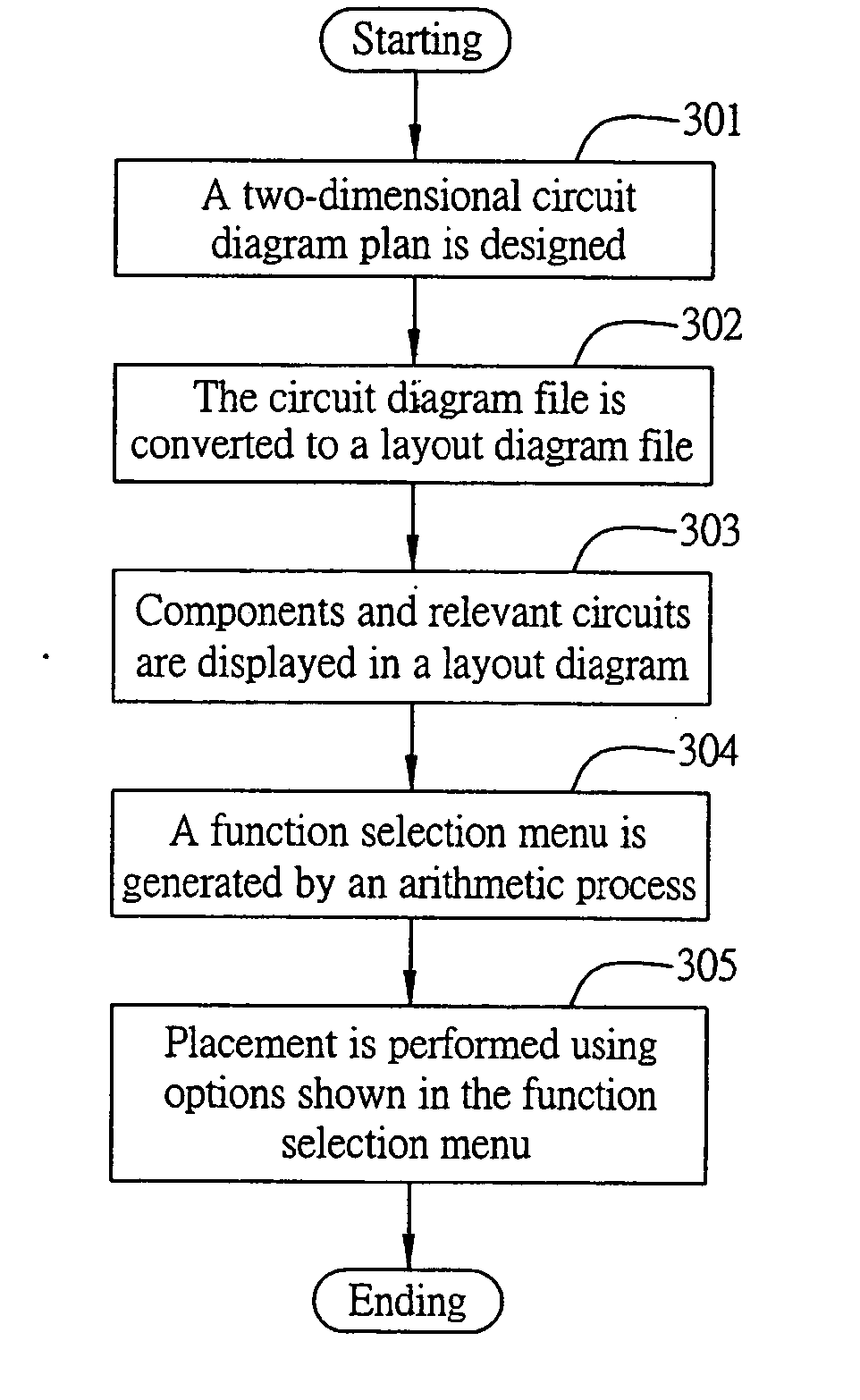
[0020]FIG. 3 is a flowchart showing a method for improving efficiency in laying out electronic components according to the present invention. In the present embodiment, the method proposed in the present invention is applied to the layout operation for electronic components via a Mentor drafting software platform (hereinafter known as the drafting software platform) included in an information processing system. Thus, when designing an electronic product, a circuit designer is able to successfully design and layout a printed circuit board for the electronic product using the method disclosed in the present invention. As shown in the diagram, in Step 301, a two-dimensional circuit diagram plan for the electronic product is designed by an electronic...


PUM


Abstract

A method is proposed for improving the layout efficiency in laying out electronic components, which is applicable to information processing equipment, to accelerate the layout of electronic components. First, a first two-dimensional plan view including various electronic component members is preset using a drafting software platform. Subsequently, the two-dimensional plan view is converted to a text file and all the relevant data of the electronic components contained in the two-dimensional plan view are encoded in the text file. Then, all of the electronic component members contained in the first two-dimensional plan view are displayed in a second two-dimensional plan view, and a function selection menu is generated by an arithmetic process. Therewith, a user is able to select the data of the electronic component contained in the text file via the function selection menu to perform the layout operations for a printed circuit board.

Description

FIELD OF THE INVENTION [0001] The present invention relates to a technique of laying out electronic components, and more particularly, to a method for improving efficiency in laying out electronic components which facilitates a user to select a desired electronic component number, so as to improve speed of laying out an electronic circuit. BACKGROUND OF THE INVENTION [0002] With a booming development of electrical technology, electronic products, such as mobile phone, digital camera, computers, and MP3 player have become popular in every family. However, a fabrication of printed circuit boards (PCBs) for the electronic products, which fabrication involves designing, circuit drafting, mechanical drafting, component placement, and drafting of a layout diagram for the printed circuit board, before fabrication of electronic products, is time-consuming. Accordingly, manufacturers continue to propose new techniques in hope of simplify the process of researching for the electronic products...

Claims


Application Information

Patent Timeline
Patent Type & Authority Applications(United States)
IPC IPC(8): G06F17/50G06F9/45
CPCG06F17/5072G06F30/392
Inventor CHANG, VAMLIN, MING-HUI
Owner INVENTEC CORP
Why Eureka
Try Eureka