Piezoelectric oscillator, manufacturing method thereof, and electronic device

a manufacturing method and piezoelectric technology, applied in the direction of oscillation generators, solid-state devices, generators/motors, etc., can solve the problems of reducing the joining strength, piezoelectric oscillator loosening at the portion, and increasing the planar size, so as to reduce the number of ic types, reduce manufacturing costs and the cost of the completed product, and reduce the planar size of the piezoelectric oscillator

Inactive Publication Date: 2006-10-26
INTELLECTUAL KEYSTONE TECH LLC
View PDF10 Cites 14 Cited by
  • Summary
  • Abstract
  • Description
  • Claims
  • Application Information

AI Technical Summary

Benefits of technology

[0010] In order to achieve the above, the piezoelectric oscillator according to an aspect of the present invention is a piezoelectric oscillator having a plurality of leads formed of one or more lead frames, terminals, which are formed on the plurality of leads and distanced one from another, are arrayed in multiple tiers in the vertical direction of a package. Due to an aspect of the present invention being configured thus, the terminals do not need to be arrayed in planar fashion since the terminals are arrayed in multiple tiers in the vertical direction of the package. This enables the planar size to be reduced, and the size thereof to be reduced.
[0011] Also, with the piezoelectric oscillator including as the terminals at least connection terminals to connect with a piezoelectric resonator and mounting terminals to mount to a mounting board, the piezoelectric resonator formed by sealing a piezoelectric resonator element within a resonator package is mounted on the connection terminals, an IC forming an oscillating circuit being mounted on the lead frame, and the lead frame and the piezoelectric resonator being sealed within the package, such that the principal surface of the mounting terminals are exposed outwards, thereby forming a resin package. In this case, good-quality piezoelectric resonators and good-quality ICs can be combined to form the piezoelectric oscillator, by adjusting the frequency of the piezoelectric resonator and checking the operation of the IC, before mounting the piezoelectric resonator on the lead frame. This reduces or prevents wasting good ICs, thereby enhancing the yield of ICs, and reducing manufacturing costs.
[0012] Further, the configuration has the entirety of the lead frame and the piezoelectric resonator sealed with resin, so even in the event that the combination of the piezoelectric resonator and IC type changes, the same resin molding mold can be used. Accordingly, small lots of a great number of types can be handled. Also, the entirety of the lead frame and the piezoelectric resonator can be insulated, also reducing or preventing intrusion of foreign matter and moisture. Accordingly, electric and chemical failure can be reduced or prevented.

Problems solved by technology

Accordingly, the smaller the piezoelectric oscillators become, the smaller the area of contact between the mounting terminals and the mounting board becomes, reducing the joining strength.
Accordingly, in the event that the piezoelectric oscillator is mounted in a portable electronic device such as a cellular telephone or the like, there is an increased probability that dropping the device may result in the piezoelectric oscillator coming loose at the portion of contact with the mounting board due to the great shock.
However, with the above-described piezoelectric oscillator, there is the problem that the planar size increases, since the connection leads need to be disposed at the intermediate portion of the mounting leads.
Consequently, there is a limit to reduction in the size of the piezoelectric oscillator.

Method used


Image

  • Piezoelectric oscillator, manufacturing method thereof, and electronic device
  • Piezoelectric oscillator, manufacturing method thereof, and electronic device
  • Piezoelectric oscillator, manufacturing method thereof, and electronic device

Examples


first exemplary embodiment

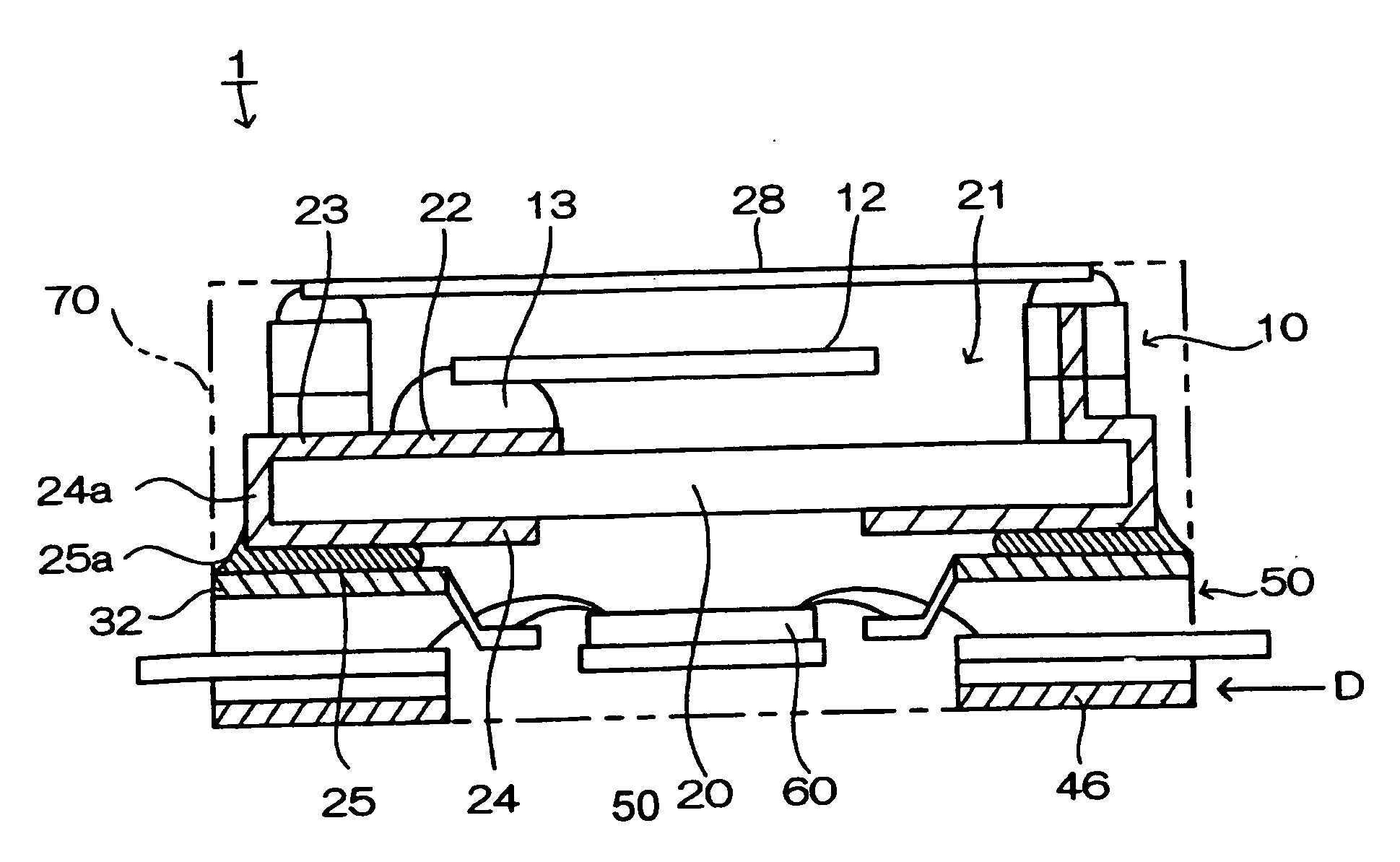
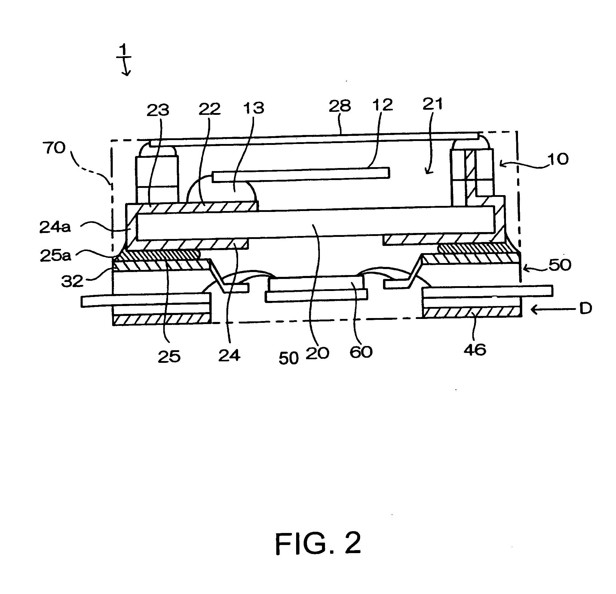
[0095] Now, before mounting the piezoelectric resonator 10 to the layered lead frame 50, the piezoelectric resonator 10 is subjected to frequency adjustment and a check of the operations of the IC 60. This allows a good piezoelectric resonator 10 and a good IC 60 to be combined to form the piezoelectric oscillator. Note that with piezoelectric oscillator types, the IC being first mounted within the package and the piezoelectric resonator element being mounted above this, defects on the piezoelectric resonator element may be discovered at the stage of adjusting the frequency following mounting of the piezoelectric resonator element. In this case, the good IC must be discarded along with the defective piezoelectric resonator element. From this point, with the first exemplary embodiment, good ICs are not discarded, so the yield of ICs is enhanced, and manufacturing costs can be reduced.

[0096] The piezoelectric resonator 10 is then mounted to the layered lead frame 50. Specifically, the...

second exemplary embodiment

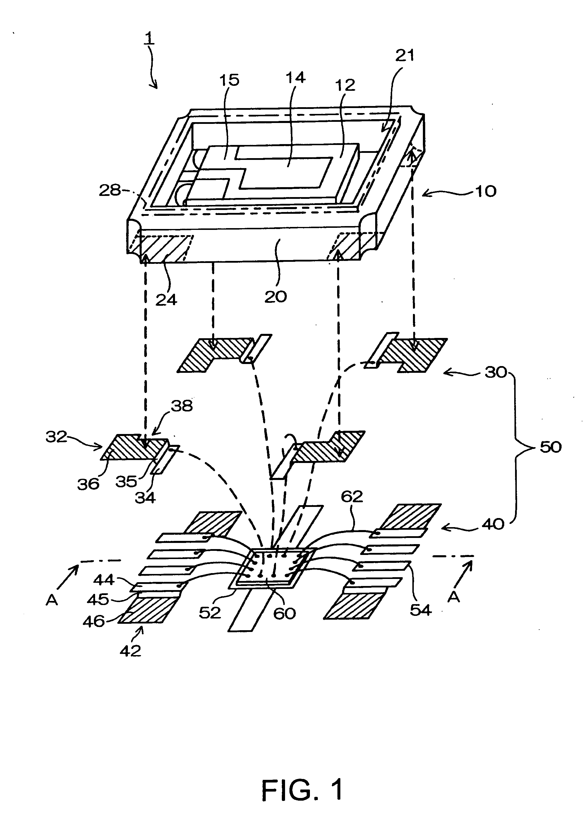
[0109]FIG. 7 illustrates a perspective view of the piezoelectric oscillator in a disassembled state. In the second exemplary embodiment as well, two lead frames 130 and 140 are overlaid to form the layered lead frame 150. Connection leads 132 are formed at the four sides of the upper lead frame 130, and the outer side portions thereof are erected upwards to form connection terminals 136. Wiring leads 152 are formed at the intermediate portion of the connection leads 132 in the depth-wise direction in FIG. 7. The outer side portions of the wiring leads 152 are erected upwards to form wiring terminals 156. Note that with the second exemplary embodiment, two wiring terminals 156 are formed in array at the intermediate portion of the connection terminals 136. On the other hand, mounting leads 142 are formed at the four sides of the lower lead frame 140, and the outer side portions thereof are erected downwards to form mounting terminals 146.

[0110] On the other hand, external electrodes...

eighth exemplary embodiment

[0145]FIG. 29 is an explanatory schematic of an As shown in FIG. 29(A), with the piezoelectric oscillator 350 according to the eighth exemplary embodiment, four mounting terminals 352 and multiple (four, in the case of the embodiment) adjusting terminals 354 are provided on the bottom face of the resin package 70, so as to be joined to (mounted on) a mounting board not shown in this figure. The sides of the adjusting terminals 354 may be exposed from the resin package 70, as with the mounting terminals 352 as shown in (B) in the figure. With the piezoelectric oscillator 350 arranged thus, the adjusting terminals 354 are joined to dummy terminals or the like provided on the mounting board by solder or the like. Accordingly, the piezoelectric oscillator 350 is joined with the mounting board by the mounting terminals 352 and the adjusting terminals 354, whereby the mounting strength is enhanced, and shock resistance can be greatly enhanced.

[0146]FIG. 30 is an explanatory diagram of a ...


PUM


Abstract

To provide a piezoelectric oscillator which can be reduced in size by reducing the planar size. With regard to a layered lead frame comprising two lead frames and, connection leads for connection with a piezoelectric resonator are formed on the upper lead frame and the connection leads are erected upwards so as to form connection terminals, and mounting leads for mounting to a mounting board are formed on the lower lead frame and the mounting leads are erected downwards so as to form mounting terminals, and an IC forming an oscillating circuit is mounted on the layered lead frame, the piezoelectric resonator formed by sealing a piezoelectric resonator element within a package is mounted on the layered lead frame, and the layered lead frame and the piezoelectric resonator are sealed within a resin package such that the principal surface of the mounting terminals are exposed outwards, thereby forming a completed article.

Description

[0001] This is a Division of application Ser. No. 10 / 729,101 filed Dec. 8, 2003. The disclosure of the prior application is hereby incorporated by reference herein in its entirety.BACKGROUND OF THE INVENTION [0002] 1. Field of Invention [0003] The present invention relates to a piezoelectric oscillator, a manufacturing method thereof, and an electronic device. [0004] 2. Description of Related Art [0005] Piezoelectric oscillators are widely used to obtain constant frequency signals in electric circuits. Japanese Examined Utility Model Registration Application Publication No. 5-16724 describes a related art piezoelectric oscillator 501 shown in FIG. 9. Note that FIG. 9(A) is a plan view partway through manufacturing, and FIG. 9(B) is a side cross-sectional diagram at a portion equivalent to the plane H-H in FIG. 9(A). With the piezoelectric oscillator 501 shown in FIG. 9(B), a piezoelectric resonator 510 is mounted on the lower face of a lead frame 530, an integrated circuit device (I...

Claims


Application Information

Patent Timeline
Patent Type & Authority Applications(United States)
IPC IPC(8): H01L41/053H03B5/32H01L25/16H03H3/02H03H9/02H03H9/05H03H9/10
CPCH01L2224/48091H01L2224/48247H03H9/1021H03H9/1014H03H9/0547H01L2924/19041H01L2224/49109H01L2924/01077H01L2924/01078H01L2924/1532H01L2924/00014H01L2924/00H01L2924/181H01L2924/00012
Inventor KOYAMA, YUGOMIYAZAKI, KATSUHIKOSHIMODAIRA, KAZUHIKONAKAJIMA, YUKARI
Owner INTELLECTUAL KEYSTONE TECH LLC
Why Eureka
Try Eureka