

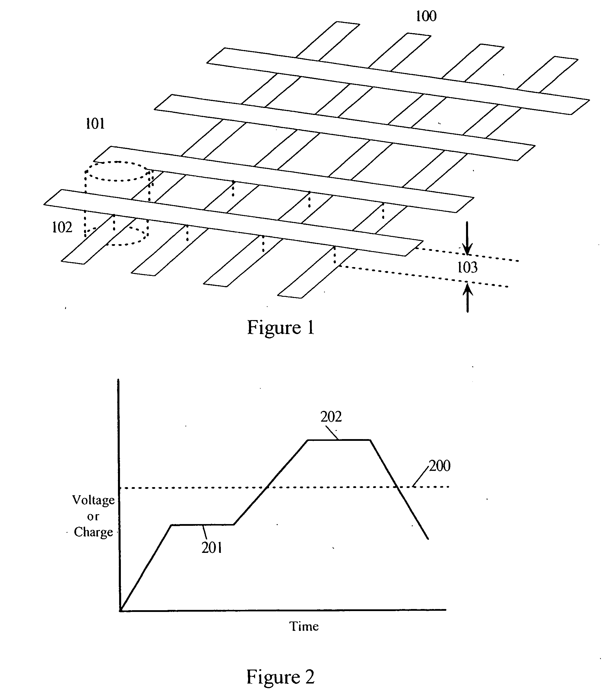
Simple matrix addressing in a display
a simple, matrix-based technology, applied in static indicating devices, liquid/fluent solid measurements, instruments, etc., can solve the problems of inconvenient high-resolution and/or video display applications, low quality of passive matrix displays, and complex active matrix displays, and achieve large electrically controlled resistance shifts.
- Summary
- Abstract
- Description
- Claims
- Application Information
AI Technical Summary
Benefits of technology
Problems solved by technology
Method used
Image

Examples
Embodiment Construction
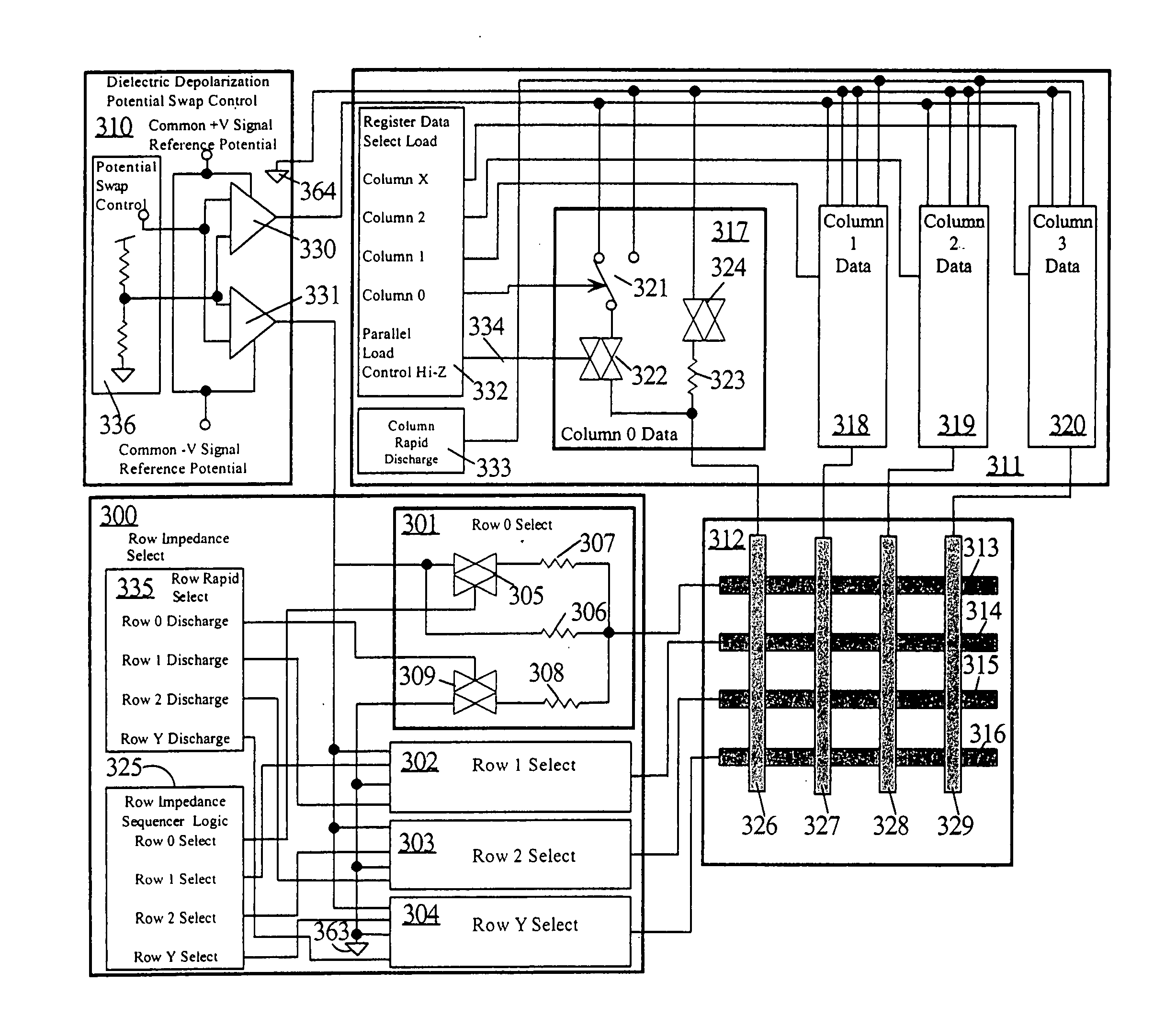
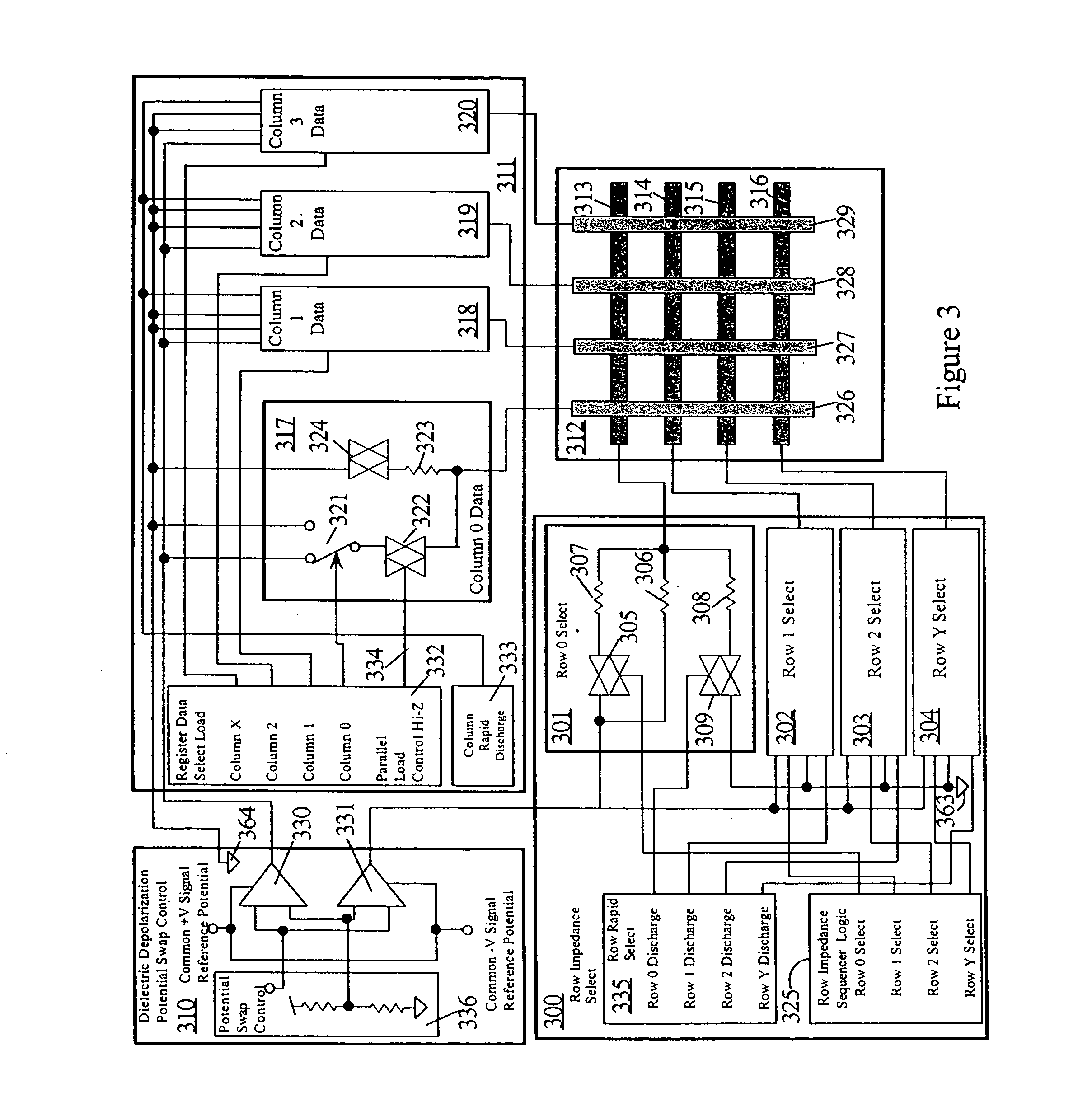
[0034] Two different embodiments of the present invention are disclosed in the detail description section. In both embodiments, impedance control is exerted upon the rows of a matrix-addressable display, with the selected row exhibiting a low in-line impedance and unselected rows exhibiting high in-line impedances. State changes in the device occur on a selected row, while no effective stage changes are intended to occur on the remaining unselected rows. The driver system scans all the rows (presumably in sequence, although this is not an intrinsic requirement), re-articulating which row shall be the lone row exhibiting a low impedance value, then moving on to the next row to be so “selected,” setting the previously selected row back into a high impedance state, and thereafter repeating this process cyclically for each row in the matrix. It should be understood that the terms “rows” and “columns” represent arbitrarily assigned labels to distinguish the two sets of lines that compose...
PUM
| Property | Measurement | Unit |
|---|---|---|
| voltage | aaaaa | aaaaa |
| distance | aaaaa | aaaaa |
| resistance | aaaaa | aaaaa |
Abstract
Description
Claims
Application Information