Semiconductor memory device

a semiconductor and memory device technology, applied in the direction of digital transmission, unauthorized memory use protection, instruments, etc., can solve the problems of increasing the putting a burden on the system side additionally, and unable to output stored data or erroneous data, etc., to achieve high-efficiency circuit constitution

Inactive Publication Date: 2006-10-26
SHARP KK
View PDF4 Cites 20 Cited by
  • Summary
  • Abstract
  • Description
  • Claims
  • Application Information

AI Technical Summary

Benefits of technology

[0013] The present invention was made in view of the above problem and it is an object of the present invention to provide a nonvolatile semiconductor memory device having a password protection function in which data cannot be read out without a cancel operation using a password, in which the password protection function is ensured after a predetermined operation such as a reset operation and great flexibility is provided for the password protection function.
[0030] According to the nonvolatile semiconductor memory device having the above characteristics, since when both of the first state specified value and the second state specified value are in the set state, the password protection function is enabled and when at least the second state specified value is in the reset state, the password protection function is disabled and only when the password is correctly inputted, the cancel operation to set the second state specified value to the reset state can be performed, the password protection function in which data cannot be read out without the cancel operation using the password can be concretely implemented. In addition, since the password protection function can be enabled or disabled using the first state specified value and the second state specified value according to the states (the set state and the reset state) of the first state specified value and the second state specified value, when the second state specified value is in the reset state and the password protection function is disabled, the state can be varied according to the first state specified value. As a result, high flexibility can be implemented in the password protection function.
[0033] Furthermore, according to the nonvolatile semiconductor memory device having the above second characteristics, since the data in the memory block in which the permanent data protection flag is set can be permanently protected from writing and erasing and can be read even when the password protection function is enabled, the memory block in which the permanent data protection flag is set can be selectively separated from the password protection function. Thus, when the nonvolatile semiconductor memory device having the second characteristics is applied to a system using the conventional nonvolatile semiconductor memory device having the permanent data protection function, the password protection function can be forcedly canceled in a certain memory block without adding a special function or circuit to the system side. Especially, in a case where the nonvolatile semiconductor memory device comprises the plurality of memory blocks, when the permanent data protection flag is set in a specific memory block and the memory block is selected as the boot-block used for a program loading access at the time of booting of the CPU, the data of the boot-block can be read out without the password. In addition, since a substantial function in which the data of the boot-block is permanently protected from writing and erasing can be implemented at the same time, there can be provided a high efficient circuit constitution.

Problems solved by technology

Thus, a password is inputted from outside before the internal data is read and when the password does not coincide with the verifying data stored in the memory device, the stored data cannot be outputted or erroneous data is outputted.
However, this trap address places a burden on the system side additionally.
For example, since the trap address is provided, when a normal serial address space is sequentially read out, it is necessary to avoid the trap address, which increases the burden on the system side.
Furthermore, according to a constitution in which data is erased in order to protect the data such as the password stored in the password region, when the password region is not appropriately accessed, the data could be lost improperly, and address management on the system side becomes complicated.
However, according to the security function disclosed in the patent document 2, a system is not designed to correspond to such selective operation.
In addition, after the protection state with the password is cancelled once, when a forced reset by turning off a power supply or a hardware reset by a command input is generated, it is not clear how effectiveness of the password is maintained afterwards.

Method used


Image

  • Semiconductor memory device
  • Semiconductor memory device
  • Semiconductor memory device

Examples


Embodiment Construction

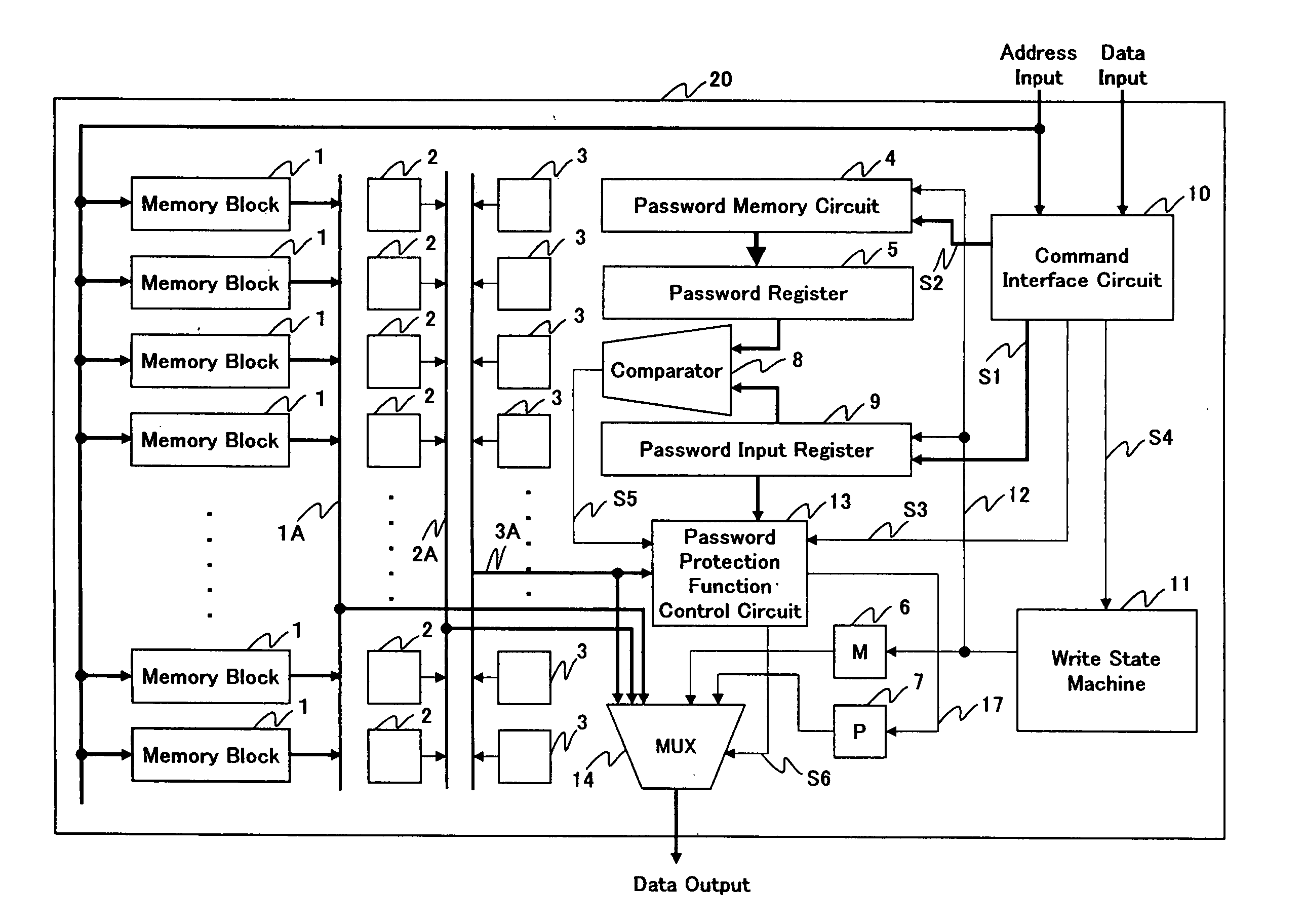
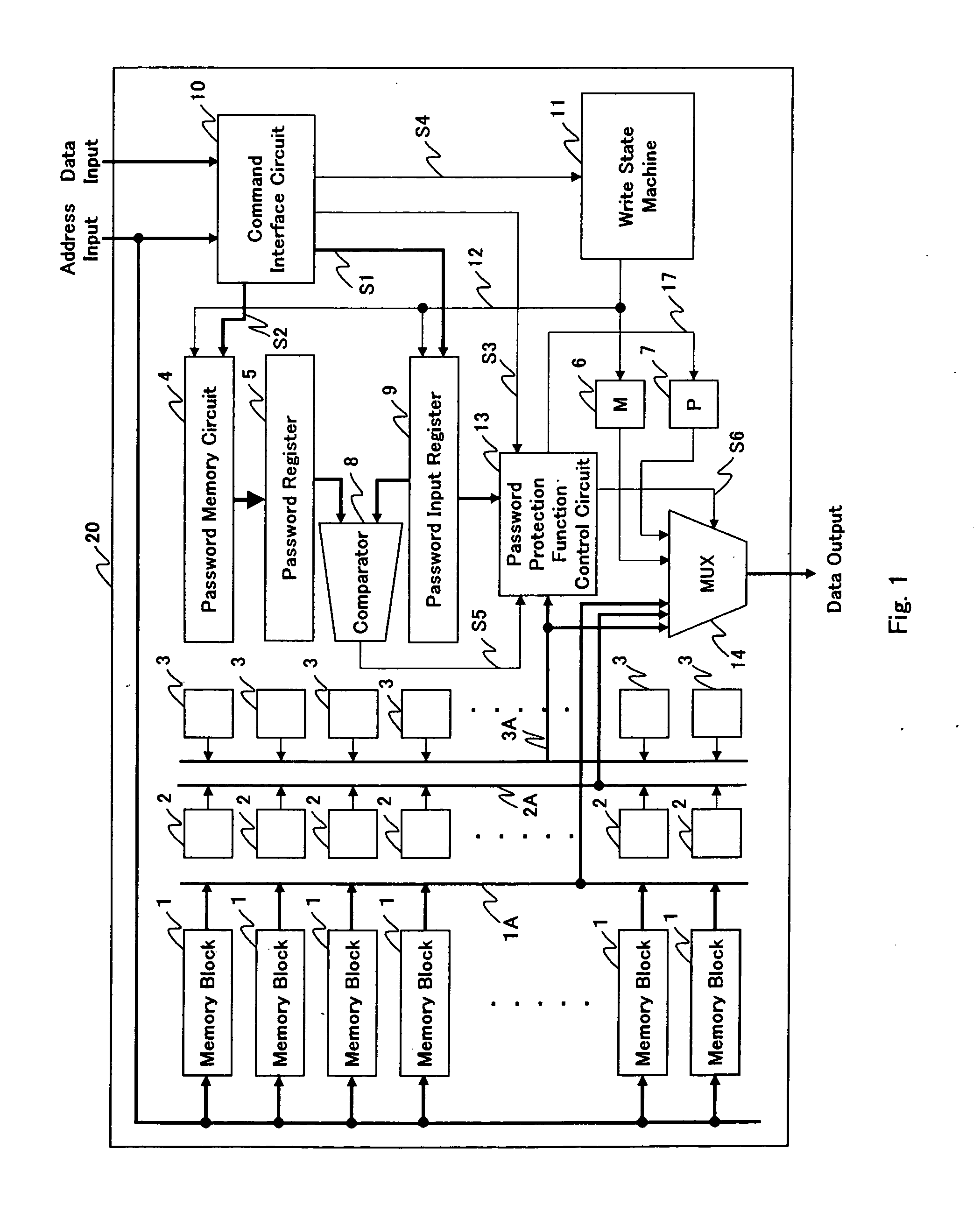
[0043] An embodiment of a nonvolatile semiconductor memory device according to the present invention (referred to as the “memory device of the present invention” hereinafter) will be described with reference to the drawings hereinafter.

[0044]FIG. 1 shows a schematic constitution of a memory device 20 of the present invention. As shown in FIG. 1, the memory device 20 of the present invention comprises a plurality of memory blocks 1, a plurality of first flag memory circuits 2, a plurality of second flag memory circuits 3, a password memory circuit 4, a password register 5, a mode bit memory circuit 6, a protection bit memory circuit 7, a comparator 8, a password input register 9, a command interface circuit 10, a write state machine 11, a password protection function control circuit 13, and a multiplexer (MUX) 14.

[0045] The memory block 1 comprises a plurality of nonvolatile memory cells arranged in matrixes of rows and columns, and it is a minimum unit in which batch erase of the ...


PUM


Abstract

In a nonvolatile semiconductor memory device according to the present invention, a password protection function is enabled or disabled based on a first specified value M and a second state specified value P such that when both of the first specified value M and the second state specified value P are in a set state, the password protection function is enabled and when at least the second specified value P is in a reset state, the password protection function is disabled, and the first state specified value M maintains a previous state and the second state specified value P follows the state of the first state specified value M in response to a reset operation, and the cancel operation to shift the second state specified value P to the reset state can be performed only when the password is inputted correctly.

Description

CROSS REFERENCE TO RELATED APPLICATION [0001] This Nonprovisional application claims priority under 35 U.S.C. §119(a) on Patent Application No. 2005-123153 filed in Japan on Apr. 21, 2005, the entire contents of which are hereby incorporated by reference. BACKGROUND OF THE INVENTION [0002] 1. Field of the Invention [0003] The present invention relates to a nonvolatile semiconductor memory device having a security function and more particularly to a nonvolatile semiconductor memory device comprising at least one memory block comprising a plurality of nonvolatile memory cells, and having a password protection function by which data cannot be read out from a part of the memory block or the entire memory block without a cancel operation using a password. [0004] 2. Description of the Related Art [0005] As the number of kinds of electronic devices using a nonvolatile semiconductor memory device is increased, usage of the nonvolatile semiconductor memory device such as a flash memory in wh...

Claims


Application Information

Patent Timeline
Patent Type & Authority Applications(United States)
IPC IPC(8): H04L9/00G06F21/60G06F21/62
CPCG06F21/79G06F12/1433G06F12/14G06F12/16
Inventor ISHIDA, TERUFUMI
Owner SHARP KK
Why Eureka
Try Eureka