CMP slurry for metallic film, polishing method and method of manufacturing semiconductor device

Active Publication Date: 2006-11-02
KIOXIA CORP
View PDF16 Cites 67 Cited by
  • Summary
  • Abstract
  • Description
  • Claims
  • Application Information

AI Technical Summary

Benefits of technology

[0008] A CMP slurry for metallic film according to one aspect of the present invention comprises water; 0.01 to 0.3 wt %, based on a total quantity of the slurry, of polyvinylpyrrolidone having a weight average molecular weight of 20,000 or more; an oxidizing

Problems solved by technology

When a Low-k material is to be employed as an insulating film, the peeling of film or the fracture of film itself would occur if the polishing friction is large.
Therefore, it is now becoming difficult to employ the conventional CMP slurry which is inherently large in polishing friction.
Since the conventional silicone-based surfactant acts strongly on silica employed an abrasive particle to generate coarse particles thereof, it is difficult to suppress the g

Method used


Image

  • CMP slurry for metallic film, polishing method and method of manufacturing semiconductor device
  • CMP slurry for metallic film, polishing method and method of manufacturing semiconductor device
  • CMP slurry for metallic film, polishing method and method of manufacturing semiconductor device

Examples


embodiment 1

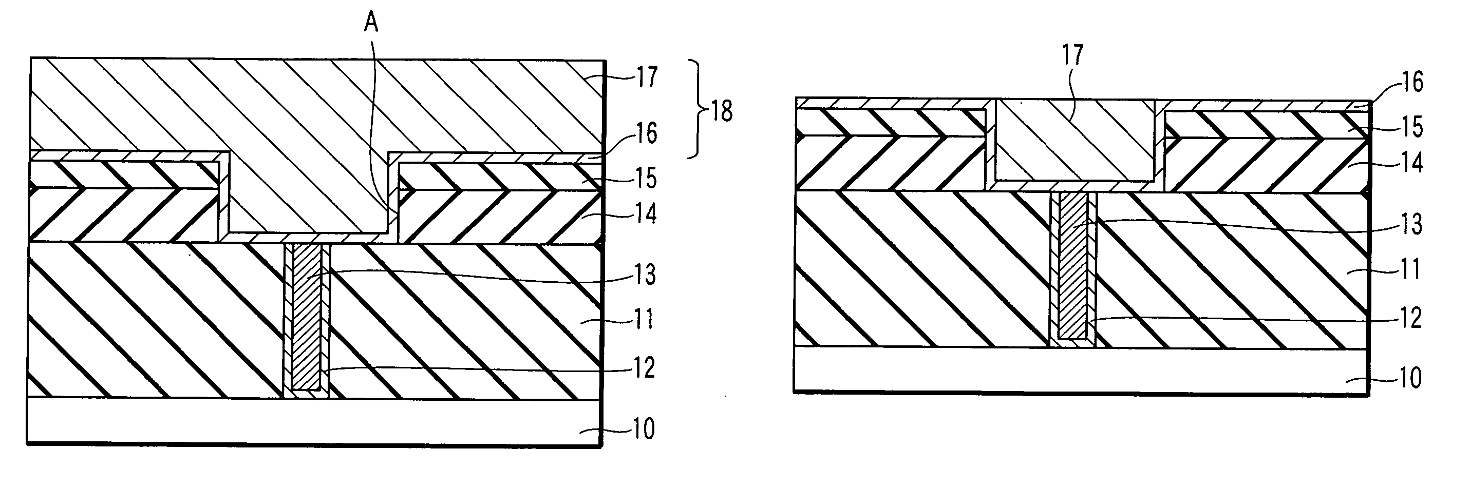
[0038] Next, this embodiment will be explained with reference to FIGS. 1 and 2.

[0039] First of all, as shown in FIG. 1, an insulating film 11 of SiO2 was formed on a semiconductor substrate 10 having a semiconductor element (not shown) formed thereon and a plug 13 was formed with a barrier metal 12 being interposed between the insulating film 11 and the plug 13. The barrier metal 12 was formed using TiN and the plug 13 was formed using W as a material therefor. Then, on these insulating film 11 and plug 13, a first low dielectric constant insulating film 14 and a second low dielectric constant insulating film 15 were successively deposited to form a laminated insulating film. This first low dielectric constant insulating film 14 can be constituted by a low dielectric constant insulating material exhibiting a relative dielectric constant of less than 2.5. For example, this first low dielectric constant insulating film 11 can be formed by at least one selected from the group consisti...

embodiment 2

[0066] By using the stock solution of slurry prepared in the aforementioned Embodiment 1 and by mixing PVPs differing in weight average molecular weight at mixing ratios shown in the following Table 4, the slurries of Nos. 16-50 were prepared.

TABLE 4MolecularContentNo.weight(wt %)1610,0000.01170.03180.05190.1200.3210.5220.72320,0000.01240.03250.05260.1270.3280.5290.73040,0000.01310.03320.05330.1340.3350.5360.737100,0000.01380.03390.05400.1410.3420.5430.744200,0000.01450.03460.05470.1480.3490.5500.7

[0067] By using each of slurries, the polishing of the Cu film was performed under the same conditions described in Embodiment 1, thereby investigating the polishing rate of Cu, the stop of CMP, the electric current of table motor, the dishing of Cu, and the corrosion of Cu.

[0068] The corrosion of Cu was evaluated such that a sample having not more than 10 portions of Cu corrosion per 1 cm2 was marked by a symbol of “◯” and a sample having more than 10 portions of Cu corrosion per 1 cm2...

embodiment 3

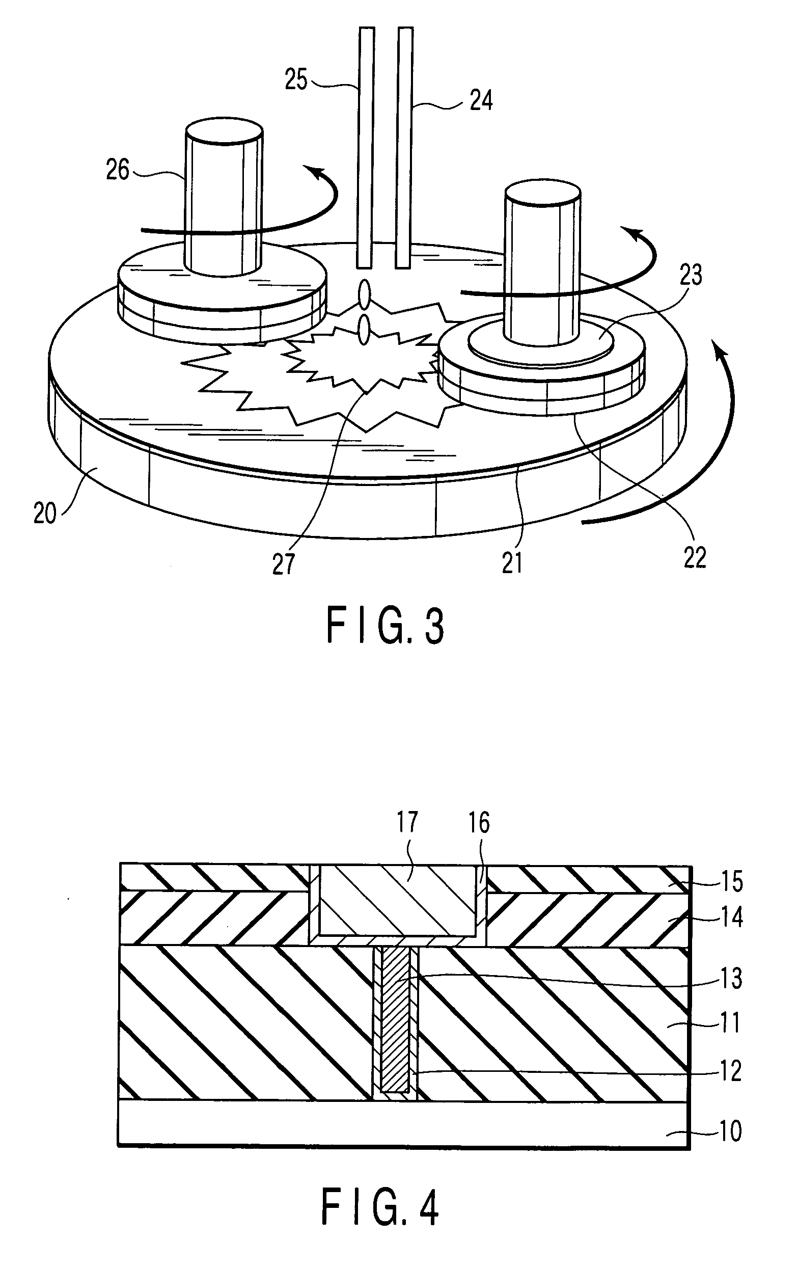
[0080] Next, this embodiment will be explained with reference to FIGS. 2 and 4.

[0081] First of all, by using the same materials as employed in the aforementioned Embodiment 1, insulating film, etc., each having the same thickness as that of Embodiment 1, were deposited to obtain a structure as shown in FIG. 1. Thereafter, a first polishing was performed using the slurry of No. 33 under the conditions specified in Embodiment 2 to expose the surface of the barrier metal 16 as shown in FIG. 2. Further, a second polishing (touch-up CMP) was performed to expose the surface of the second low dielectric constant insulating film 15 as shown in FIG. 4.

[0082] The touch-up CMP was performed as follows. Namely, first of all, as shown FIG. 3, while rotating a turntable 20 having a polishing pad 21 attached thereto at a speed of 100 rpm, a top ring 23 holding a semiconductor substrate 22 was allowed to contact with the turntable 20 at a polishing load of 200 gf / cm2. The rotational speed of the ...


PUM

PropertyMeasurementUnit
Forceaaaaaaaaaa
Viscosityaaaaaaaaaa
Nanoscale particle sizeaaaaaaaaaa

Abstract

A CMP slurry for metallic film is provided, which includes water, 0.01 to 0.3 wt %, based on a total quantity of the slurry, of polyvinylpyrrolidone having a weight average molecular weight of not less than 20,000, an oxidizing agent, a protective film-forming agent containing a first complexing agent for forming a water-insoluble complex and a second complexing agent for forming a water-soluble complex, and colloidal silica having a primary particle diameter ranging from 5 to 50 nm.

Description

CROSS-REFERENCE TO RELATED APPLICATIONS [0001] This application is based upon and claims the benefit of priority from prior Japanese Patent Application No. 2005-132095, filed Apr. 28, 2005, the entire contents of which are incorporated herein by reference. BACKGROUND OF THE INVENTION [0002] 1. Field of the Invention [0003] This invention relates to a slurry for chemical mechanical polishing (CMP), a polishing method, and a method of manufacturing a semiconductor device. In particular, this invention relates to a CMP slurry for metallic film, a polishing method of a metallic film, and a method for manufacturing a semiconductor device using a damascene wiring. [0004] 2. Description of the Related Art [0005] A Cu damascene wiring to be mounted on a high-performance LSI has been formed by using CMP. In this CMP, the polishing is performed in two steps, i.e., a first polishing where the abrasion of Cu is mainly performed, and a second polishing where the abrasion of redundant metal and i...

Claims


Application Information

Patent Timeline
IPC IPC(8): C09K13/00H01L21/461B44C1/22H01L21/302B24B37/00B82Y10/00B82Y99/00C09K3/14H01L21/304
CPCC09G1/02H01L22/26H01L21/3212C09K3/1463
Inventor MINAMIHABA, GAKUFUKUSHIMA, DAIKURASHIMA, NOBUYUKIYAMAMOTO, SUSUMUYANO, HIROYUKI
Owner KIOXIA CORP
Why Eureka
Try Eureka