Amorphous optical coupling structure for an electromagnetic wave detector and associated detector

a detector and optical coupling technology, applied in the field of electromagnetic wave detectors, can solve the problems of limiting the use of these devices to a very narrow absorption window, and achieve the effect of effective optical coupling and elimination of periodic effects

Inactive Publication Date: 2006-11-02
SOFRADIR
View PDF28 Cites 12 Cited by
  • Summary
  • Abstract
  • Description
  • Claims
  • Application Information

AI Technical Summary

Benefits of technology

[0008] This is why the present invention proposes a novel amorphous optical coupling structure designed to couple electromagnetic radiation on the surface of a photodetector, in order to eliminate the periodic effects while still ensuring effective optical coupling.

Problems solved by technology

The major drawback of the use of gratings is the wavelength and angular resonance associated with the increase in absorption, thereby limiting the use of these devices to a very narrow absorption window.

Method used


Image

  • Amorphous optical coupling structure for an electromagnetic wave detector and associated detector
  • Amorphous optical coupling structure for an electromagnetic wave detector and associated detector
  • Amorphous optical coupling structure for an electromagnetic wave detector and associated detector

Examples


first embodiment

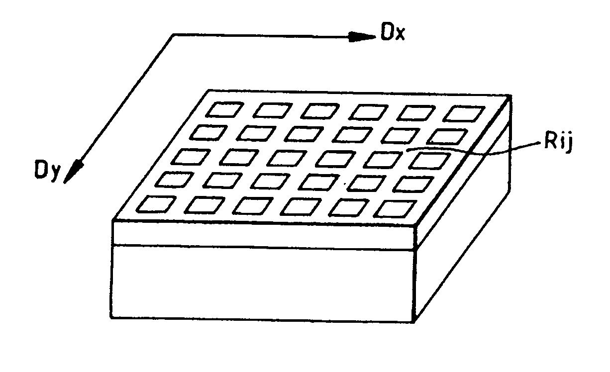
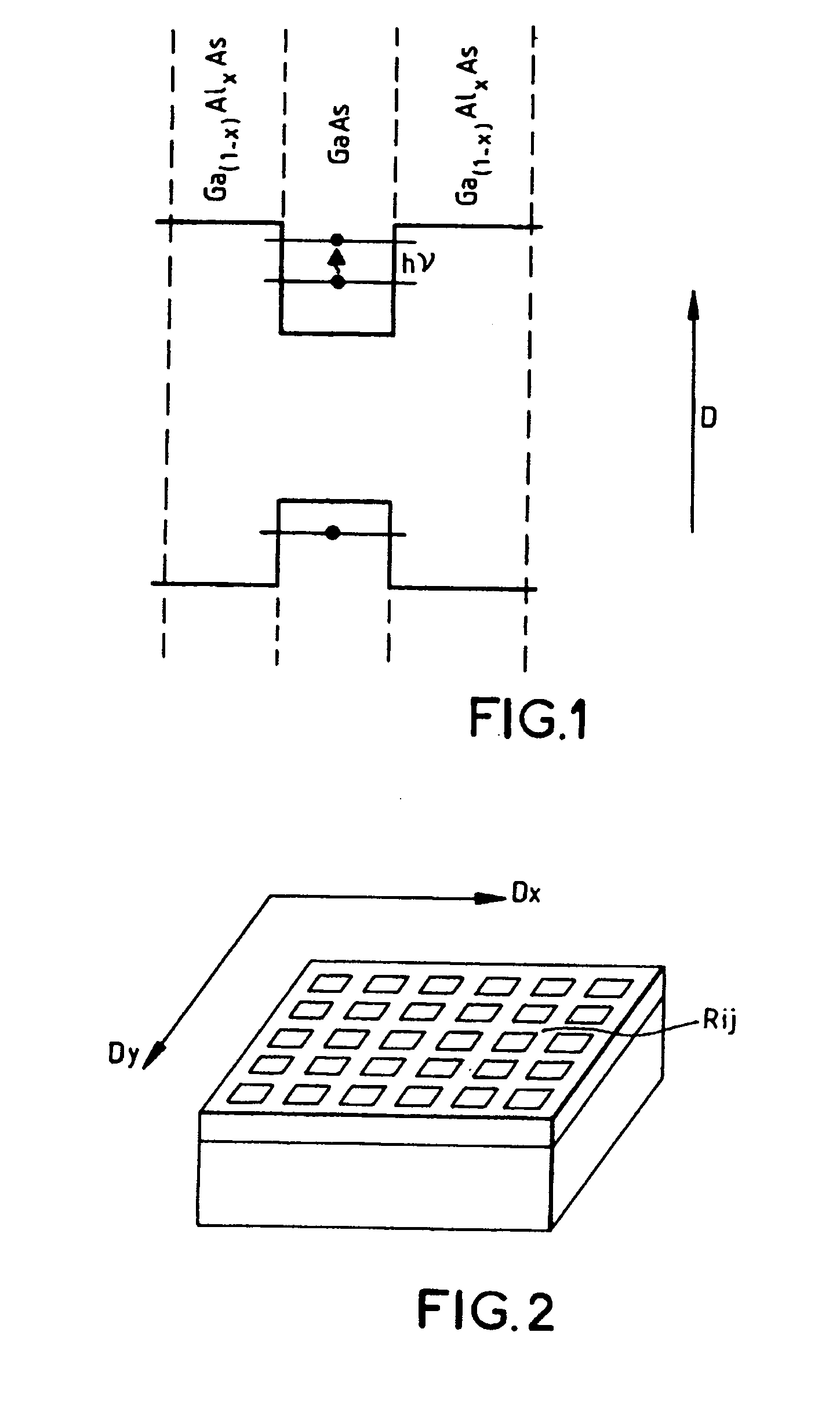
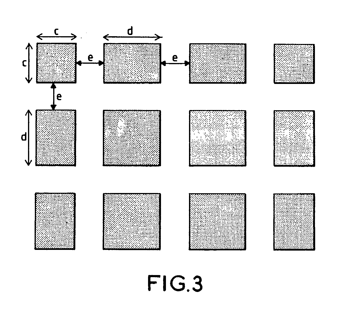
[0036] The coupling surface is made up of four series of elementary features, two series of square features having dimensions of c×c, d×d and two series of rectangular features having dimensions of c×d and d×c, as illustrated in FIG. 3. The distance between features is constant and equal to e.

[0037] The length c+e is matched to a first wavelength λ1 and the length d+e is matched to a second wavelength λ2 so as to obtain an effective coupling structure over a certain spectral band, that is to say c+e≅λ1 / n and d+e≅λ2 / n, where n is the optical index of the detector medium.

second embodiment

[0038] The optical coupling surface is defined in terms of elementary surfaces, again called elementary cells having dimensions of a×a, a×b, b×a and b×b, as illustrated in FIG. 4. In this embodiment, four series of features (M1i, M2i, M3i and M4i) homothetic with said elementary cells are employed. The features have dimensions of c×c, cM×dM, dM×cM and d×d, respectively. The dimensions cM and dM are determined so as to maintain the same fill factor as for the a×a and b×b cells.

[0039] The length a is matched to a first wavelength λ1 and the length b is matched to a second wavelength λ2 so as to obtain an effective coupling structure over a certain spectral band. For each type of cell, the feature is placed at the center of the cell, the spacing between each feature (ec+eM, eM+ed, ed+ed, etc.) being variable within the structure.

third embodiment

[0040] The optical coupling surface is defined in terms of elementary surfaces again called elementary cells having dimensions of a×a, a×b, b×a and b×b, as illustrated in FIG. 5.

[0041] In this embodiment, four series of features (M1i, M2i, M3i and M4i) homothetic with said elementary cells are employed. The features have dimensions of c×c, c×d, d×c and d×d, respectively.

[0042] The length c is matched to a first wavelength λ1 and the length d is matched to a second wavelength λ2 so as to obtain an effective coupling structure over a certain spectral band.

[0043] The fill factor is not the same between the square cells and the rectangular cells.

[0044] In general, the optical structure according to the invention may comprise etched features (the preferred embodiment as technologically this is the easiest to produce).

[0045] The detector may be conventionally produced on the surface of a substrate S made of a possibly undoped semiconductor material. An assembly of layers constituting...


PUM


Abstract

The invention relates to an optical coupling structure intended to couple electromagnetic radiation to the surface of a photodetector, wherein a coupling surface paved along mutually perpendicular first and second directions by a set of N series (M1i, M2i, . . . Mni) of first features, second features, . . . nth features, the features being identical within any one series, the features being distributed along the first and second directions, the distance between the centers of two adjacent features or the inter-reticular distances between two adjacent features being variable. The subject of the invention is also a detector or a laser source comprising said coupling structure.

Description

FIELD OF THE INVENTION [0001] The field of the invention is that of electromagnetic wave detectors made of semiconductor material and especially one having a multiple quantum well structure, particularly one suitable for the infrared range. BACKGROUND OF THE INVENTION [0002] The rapid advances made in epitaxial growth on GaAs-type substrates has led to the development of a new class of electromagnetic wave detectors using the absorption of radiation around a wavelength λ corresponding to the electron transition between various energy levels within one and the same band or between the valence band and the conduction band. The diagram shown in FIG. 1 illustrates this type of transition. [0003] The recent evolution in performance of this type of component is due in particular to the relatively easy production of semiconductor heterojunction multilayers in the standard system by MBE (molecular beam epitaxy), that is to say the GaAs / Ga(1-x)AlxAs. By adjusting the growth parameters, the t...

Claims


Application Information

Patent Timeline
Patent Type & Authority Applications(United States)
IPC IPC(8): H01J40/14H01L31/0232H01L31/0352
CPCB82Y20/00H01L31/035236H01L31/0232H01L31/02327
Inventor BOIS, PHILIPPEBRIERE DE L'ISLE, NADIACOSTARD, ERICDE ROSSI, ALFREDO
Owner SOFRADIR
Why Eureka
Try Eureka