Thin-film transistor

a transistor and thin film technology, applied in the field of thin film transistors, can solve the problems of reducing the mobility of the carrier, increasing the area, and reducing the aperture ra

Inactive Publication Date: 2006-11-02
IND TECH RES INST
View PDF8 Cites 6 Cited by
  • Summary
  • Abstract
  • Description
  • Claims
  • Application Information

AI Technical Summary

Benefits of technology

[0007] In view of the foregoing, an object of the invention is to provide a TFT which, through a special structure design, can avoid the undesired effects due to its intrinsic defects and the electrical property changes due to the deflection of the substrate.

Problems solved by technology

Such intrinsic defects will reduce the carrier mobility.
However, one then faces such problems as increasing area and lower aperture rate.
Therefore, the kink effect is likely to occur.
This in turn will result in the problems of a shorter lifetime and functioning instability.
This is a big engineering problem that requires a huge amount of manpower, time, and capital.
Therefore, it is not suitable for flexible circuits.
Once there is any deviation in the process, the electrical performance will be bad.
The conventional TFT structure is totally unsuitable for the above purposes.

Method used


Image

  • Thin-film transistor
  • Thin-film transistor
  • Thin-film transistor

Examples


first embodiment

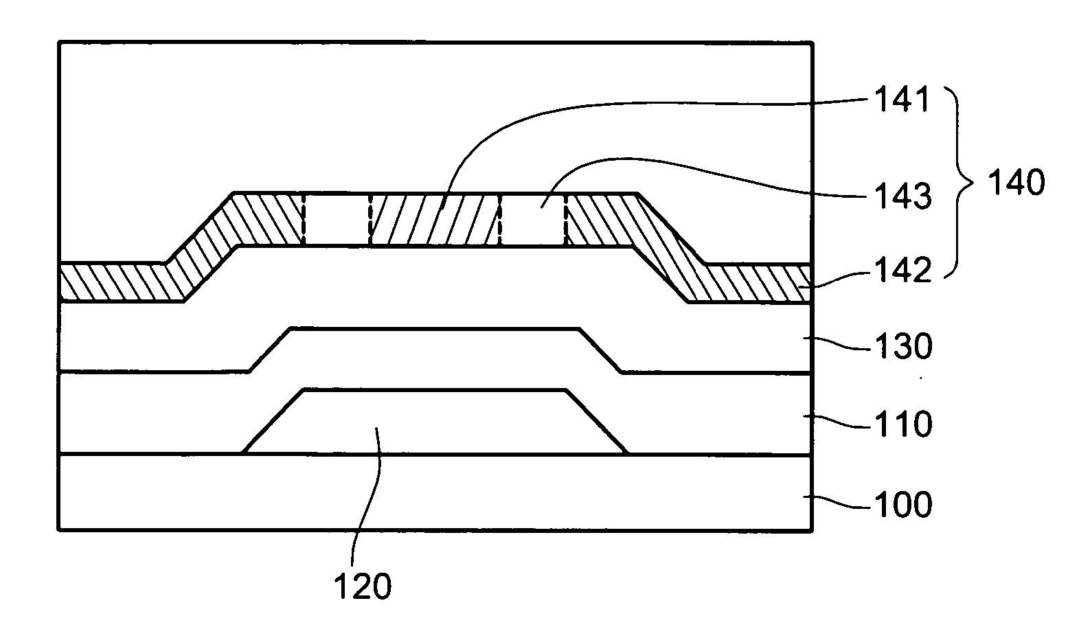
[0028]FIGS. 5A and 5B are the cross-sectional and top views of the TFT according to the invention. The TFT is an inverter staggered TFT of the bottom gate type. The flexible substrate 100 is formed with a gate layer 120. An insulating layer 110 is formed on the gate layer 120 to provide insulation. The α-Si semiconductor layer 130 is formed on the gate layer 120 and the insulating layer 110. The source / drain layer 140 is formed on the semiconductor layer 130. Besides, the disclosed TFT further contains an Ohmic contact layer between the semiconductor layer and the source / drain layer in practice. The Ohmic contact layer is the adhesive layer between the semiconductor layer and the source / drain layer, forming an Ohmic contact in between. The source / drain layer 140 contains a source 141, a drain 142, and a channel 143. The source 141 and the drain 142 are formed inside and outside a channel 143. The channel 143 is comprised of an annular band and two non-annular regions. A peninsula re...

second embodiment

[0031] As shown in FIG. 8, the channel 243 in the invention has an annular band, whose inner side defines a closed island region. The source 241 is circular, and so is the gate layer 220. This structure enables more transmission directions between the source 241 and the drain 242, achieving almost omni-directional. A higher current stability is achieved. In particular, the source 241 is provided with a wire 250 for electrically connecting to outside.

[0032] The shape of the channel 243 is not limited to annular, and the shapes of the source 241 and the drain 242 only need to match with that of the channel. The source 241 has the same shape as the island region. This is illustrated in FIGS. 9A and 9B. The island regions defined by the channels 243a, 243b, respectively, are roughly rectangular and polygonal.

[0033] The profile of the gate layer 220 corresponds to that of the island region. The area of the gate layer 220 can be either smaller or bigger than the island region. Alternativ...


PUM


Abstract

A thin-film transistor (TFT) is described to have a gate layer, an insulating layer, a semiconductor layer, and a source/drain layer formed on a flexible substrate. The source and the drain layers are separated by a channel with a special shape. This does not only increase the aspect ratio of the channel per unit area, the source and the drain also have multiple directions for transmitting carriers. The carrier mobility of the TFT is thus enhanced with uniform and stable circuit properties.

Description

BACKGROUND OF THE INVENTION [0001] 1. Field of Invention [0002] The invention relates to a TFT and, in particular, to a TFT with a special structure. [0003] 2. Related Art [0004] The active layer of the TFT is made of semiconductor materials to increase the carrier mobility. Therefore, they have been widely used in circuits of various functions. However, the active layer has grains of different sizes. Such intrinsic defects will reduce the carrier mobility. Moreover, the TFT itself requires a higher working voltage. For example, the carrier mobility of an α-Si TFT is between 0.5 cm2 / V.S and 1 cm2 / V.S, whereas that of a poly-Si TFT is between 30 cm2 / V.S and 300 cm2 / V.S [0005] Under the restriction of lower carrier mobility due to the above-mentioned intrinsic defects, it is necessary to have a sufficiently large driving current to charge pixel capacities. This can only be achieved by increasing the aspect ratio, W / L, of the channel. However, one then faces such problems as increasing...

Claims


Application Information

Patent Timeline
Patent Type & Authority Applications(United States)
IPC IPC(8): H01L29/04
CPCH01L27/1296H01L29/78603H01L29/41733
Inventor SU, KENG-LIKUNG, CHEN-PANGLIN, JAN-RUEICHANG, CHIA-PAOHUANG, YI-HSUN
Owner IND TECH RES INST
Why Eureka
Try Eureka