High power LEDs

a technology of leds and heat dissipation leads, applied in the field of leds, can solve the problems of reducing affecting the heat dissipation efficiency of leds, and reducing so as to increase the air convection efficiency and reduce the temperature of the chip. , the effect of increasing the thermal conductivity

Inactive Publication Date: 2006-11-02
IND TECH RES INST
View PDF14 Cites 25 Cited by
  • Summary
  • Abstract
  • Description
  • Claims
  • Application Information

AI Technical Summary

Benefits of technology

[0012] In the light of forgoing drawbacks, an objective of the present invention is to provide a high power LED that increases air-contact surface area and achieves high thermal conductivity and high heat convection.
[0013] Another objective of the present invention is to provide a high power LED that can be applied to small-size products.
[0014] Yet another objective of the present invention is to provide a high power LED that promotes industrial value.

Problems solved by technology

Moreover, current LED light-emitting efficiency is only 15% (external quantum efficiency), so most of the input energy converts to heat, which results in temperature rise.
The device may even fail due to overheating.
However, the contact area of the metal slug 23 and the air is limited.
However, such materials usually have a larger size.
As a result, more spaces are occupied by such larger-area element or material with high thermal conductivity for increasing the surface area with area, which hinders the application of LEDs to small-size application.
Meanwhile, since this conventional technique has to be connected to larger-sized heat dissipating substrate or using metal heat dissipating substrate or fin for heat dissipation.
Thus, additional cost is required for circuit fabrication.
However, similar to the last patent, there is no design that increases the area that contacts the air.
However, such heat dissipating design is at the rim of the whole system, it also occupies a relatively large area and is difficult to apply to small-size products.
Although the curved indentations 101 of this patent allows the surface area contacting the air to be increased, but the location of the LED chip does not provide direct contact of the LED chip with the heat dissipating element 10 and its curved indentations 101.
Moreover, in the conventional designs using heat conduction and convection for heat dissipation, larger elements or other materials with high thermal conductivity need to be added, which occupies more space and impedes smaller-size applications.

Method used


Image

  • High power LEDs
  • High power LEDs
  • High power LEDs

Examples


first embodiment

[0038] FIGS. 7 to 10 are diagrams depicting a high power LED according to a first embodiment of the present invention. As shown in FIG. 7, the high power LED 1 of this embodiment includes a porous material layer 11, a thermal conductive layer 13 and a chip 15.

[0039] The porous material layer 11 can, for example, be a porous ceramic (as shown in FIGS. 8a and 8b), roughened ceramic or metal after etching or manufacturing, oxidized film with rough surface formed by anodic treatment (as shown in FIG. 9), metal foam such as aluminum foam (as shown in FIG. 10) and other equivalent elements that acts as a substrate for a package and has a large surface area contacting the air, thereby enhancing air convection for overall heat dissipation.

[0040] The thermal conductive layer 13 is disposed on the top surface of the porous material layer 11, and can be made of materials such as copper, aluminum, graphite and other equivalent materials with high thermal conductivity and electrical conductivi...

second embodiment

[0046]FIG. 11 is a diagram depicting a high power LED according to a second embodiment of the present invention, in which, elements that are similar or the same as those in the first embodiment are denoted similar or the same symbols, and descriptions thereof are omitted.

[0047] The major difference between the first embodiment and the second embodiment is in that the high power LED 1 of the first embodiment has a double-electrode design, while the LED of the second embodiment has a multiple-electrode design.

[0048] As shown in FIG. 11, the thermal conductive layer 13 is provided with a plurality of insulating portions 133, separating the thermal conductive layer 13 into many insulated regions. In this embodiment, the insulating portions 133 separates the receiving portion 131 into five electrodes 1311, 1313, 1315, 1317 and 1319 for polycrystalline use. It should be noted that although the receiving portion 131 is separated into five electrodes 1311 to 1319 by the insulating portion...

third embodiment

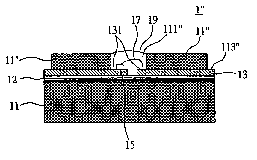
[0049]FIG. 12 is a diagram depicting a high power LED 1′ according to a third embodiment of the present invention, in which, elements that are similar or the same as those in the previous embodiments are denoted similar or the same symbols, and descriptions thereof are omitted.

[0050] The major difference between the third embodiment and the previous embodiments is in that the third embodiment is formed with a thermal conductive layer 13′ with high thermal conductivity and electrical conductivity stacked on top of the porous material layer (an insulating layer in this embodiment) made of a material such as copper, silver, gold, aluminum or other equivalent materials by thermal vapor deposition, sputtering, coating or other equivalent methods.

[0051] As shown in FIG. 12, the high power LED 1′ may also be manufactured with trace pattern for double or multiple electrodes (receiving portion 131 and insulating portion(s) 133 in the previous embodiments) by method such as a photolithograp...


PUM

PropertyMeasurementUnit
external quantum efficiencyaaaaaaaaaa
thermal conductiveaaaaaaaaaa
surface areaaaaaaaaaaa

Abstract

A high power LED has at least a porous material layer, a thermal conductive layer and a chip. The thermal conductive layer is disposed on the surface of the porous material layer and the chip is disposed on the thermal conductive layer. Heat generated by the chip is conducted from the thermal conductive layer to the porous material layer, and convected outside via the porous material layer. Thereby, surface area in contact with the air is increased and high thermal conductivity and high heat convection are also achieved.

Description

FIELD OF THE INVENTION [0001] The present invention relates to LEDs (Light Emitting Diodes), and more particularly, high-power heat-dissipating LEDs. BACKGROUND OF THE INVENTION [0002] The main principle of Light Emitting Diodes (LEDs) is by applying current to light emitting materials to achieve light emitting effect. In recent years, high-power LEDs bring LED light source applications into a whole new era. High-power LEDs are characterized by small size, high luminance of light and maximum light output per unit area, which eliminate the use of traditional LED arrays. Accordingly, the LED light source may provide better light source characteristics; and facilitate optical designs and applications. In the meantime, the small size and high luminance of the high-power LEDs open a new door for the LED light sources and also allow design of LED applications to be more flexible. Common applications include car lights, flash lights and other lighting applications with very small size and ...

Claims


Application Information

Patent Timeline
Patent Type & Authority Applications(United States)
IPC IPC(8): H01L33/00H01L33/48H01L33/60H01L33/64
CPCH01L33/483H01L33/60H01L33/641H01L33/647H01L2224/48091H01L2924/12041H01L2224/45144H01L2924/00014H01L2924/00
Inventor YANG, CHUN CHIEHCAO, HONG-XIKUO, CHIA-TAICHEN, CHIH-LICHEN, CHENG-FAHORNG, JI-BIN
Owner IND TECH RES INST
Why Eureka
Try Eureka