
Clock processing circuit

a clock processing and circuit technology, applied in the direction of generating/distributing signals, pulse techniques, instruments, etc., can solve the problem of high driving force, achieve the effect of preventing the generation of timing errors, reducing delays, and reducing the effect of characteristic variations

Inactive Publication Date: 2006-11-02
EASTMAN KODAK CO
View PDF4 Cites 4 Cited by
  • Summary
  • Abstract
  • Description
  • Claims
  • Application Information

AI Technical Summary

Benefits of technology

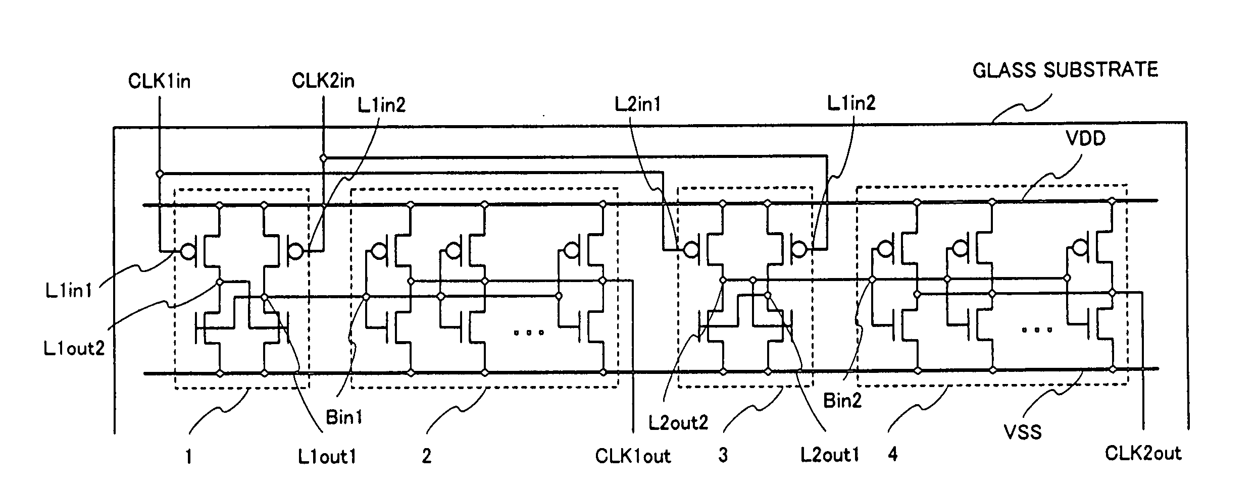
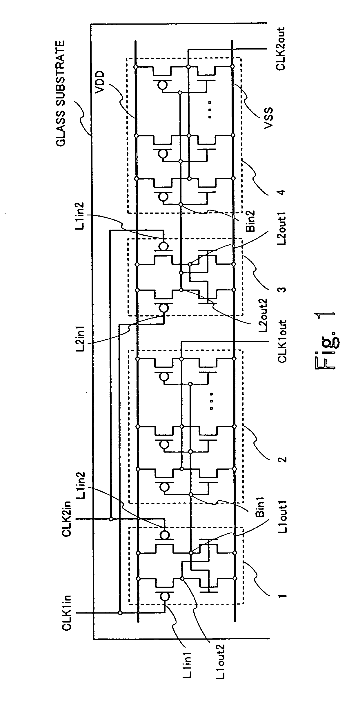
[0018] As described above, according to the present invention, clocks output from the first and second converting circuits are input to the first and second buffer circuits which are disposed adjacent to the respective first and second converting circuits, respectively. With this structure, it is possible to achieve the input path from the first converting circuit to the first buffer circuit and the input path from the second converting circuit to the second buffer circuit which are both very short and have substantially the same distance to thereby reduce a delay caused in these input paths, whereby a stabilized output clock can be obtained.
[0020] While each of the first and second converting circuits may have one input and one output, in this case, effects of characteristic variations between the two converting circuits is increased, and a pair of the output clocks are likely to be unbalanced especially when the signal level of the input signals is low. According to the present invention, each converting circuit is configured to have two inputs and two outputs, so that a stabilized operation can be achieved even when the signal level of an input signal is low.

Problems solved by technology

In general, a clock buffer circuit supplies a clock to a great number of circuits and therefore requires high driving force.
Because a clock signal output from the clock buffer is supplied to a great number of circuits, such a delay is undesirable and causes erroneous operation, especially in an application which requires a high frequency.

Method used


Image

  • Clock processing circuit
  • Clock processing circuit
  • Clock processing circuit

Examples


Embodiment Construction

[0026] A preferred embodiment of the present invention will be described in detail with reference to the accompanying drawings.

[0027]FIG. 1 shows a two-phase level shift buffer circuit which includes a first level shifter 1, a second level shifter 3, a first buffer 2, and a second buffer 4.

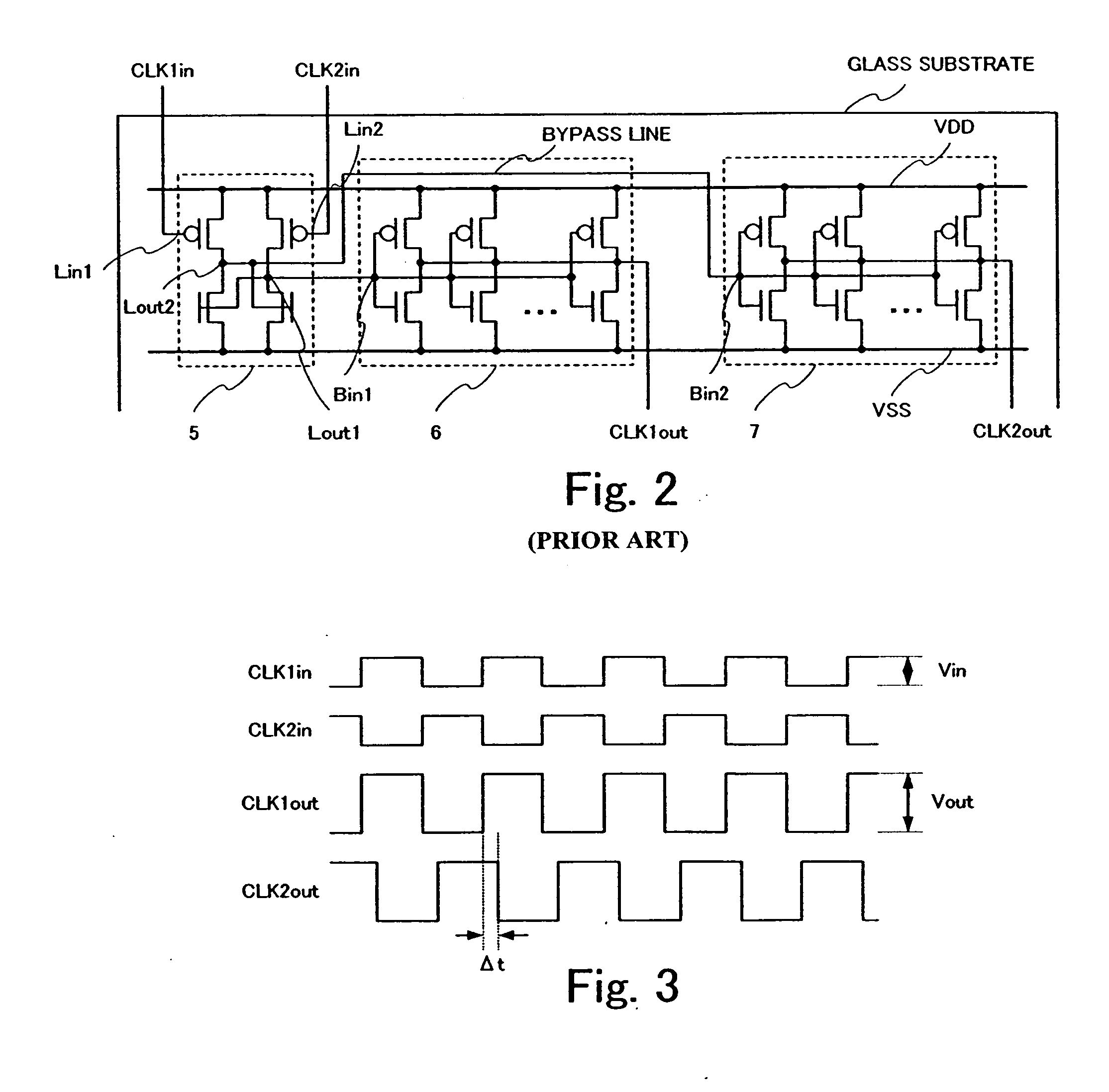
[0028] As in the related art example shown in FIG. 2, a pair of input clocks CLK1in and CLK2in having complementary phases as shown in FIG. 3 are supplied from an external IC to the two-phase level shift buffer circuit, where the input clocks are level-shifted as shown in FIG. 3 and converted into stabilized output clocks CLK1out and CLK2out, which are then output.

[0029] More specifically, the input clocks CLK1in and CLK2in are input to the first level shifter 1 having two inputs. As with the related art example shown in FIG. 2, the first level shifter 1 includes two paths each formed by a p-channel TFT and an n-channel TFT which are connected in series between a positive power source VDD (for ...


PUM


Abstract

A clock processing circuit wherein input clocks are converted into stabilized output clocks, includes a first level shifter and a second level shifter; first and second buffer circuits for producing stabilized output clocks; a first output conductive path from the first level shifter and a second output conductive path from the second level shifter provided to the first buffer and a second buffer over the first and second conductive paths respectively; and the first buffer being disposed adjacent to the first level shifter and the second buffer being disposed adjacent to the second level shifter so that the delay amount of clocks on two conductive paths is reduced and a difference in delay amounts between these clocks is reduced or suppressed.

Description

FIELD OF THE INVENTION [0001] The present invention relates to a clock processing circuit for stabilizing a pair of input clocks having complementary phases and outputting the stabilized clocks. BACKGROUND OF THE INVENTION [0002] Small size displays such as liquid crystal displays (LCDs) and organic EL displays are used in portable information terminals such as mobile phones, digital cameras, and the like, and there is a demand for further reduction in size and weight and an increase in resolution for such displays. [0003] Small size displays employing a thin film transistor (TFT) in which low temperature poly-silicon is used as an active layer are advantageous in that they can be configured to form a driver circuit and other various circuits on a glass substrate. Accordingly, in such displays using a TFT, despite their small size, various functions can be installed, thereby increasing their value as a product. [0004] Here, the various circuits formed on the glass substrate are driv...

Claims


Application Information

Patent Timeline
Patent Type & Authority Applications(United States)
IPC IPC(8): G06F1/04
CPCG06F1/04
Inventor KAWABE, KAZUYOSHI
Owner EASTMAN KODAK CO
Learn More