


Quick Research
Generate reliable direction feasibility study reports for your R&D in just a few steps.

Technical Q&A
Discover and master advanced knowledge NOW. Basics, ideas, possibilities, all at once.

Find Solutions
As an expert in R&D theories, this can generate solutions to your technical problems instantly.

Evaluate Feasibility
Analyze your overall solution with one click, know your potential R&D risks in advance.

Monitor Landscape
Get weekly tech updates, stay abreast of the latest tech innovations and key insights.
Liquid crystal device, driving method thereof, and electronic apparatus
a driving method and liquid crystal technology, applied in static indicating devices, non-linear optics, instruments, etc., can solve problems such as conspicuous problems, reduced numerical apertures, and poor alignment of liquid crystal molecules, and achieve excellent dynamic image visibility and speed. high
- Summary
- Abstract
- Description
- Claims
- Application Information
AI Technical Summary
Benefits of technology
Problems solved by technology
Method used
Image

Examples
first embodiment
[0056] First, a liquid crystal device according to a first embodiment of the invention will be described.
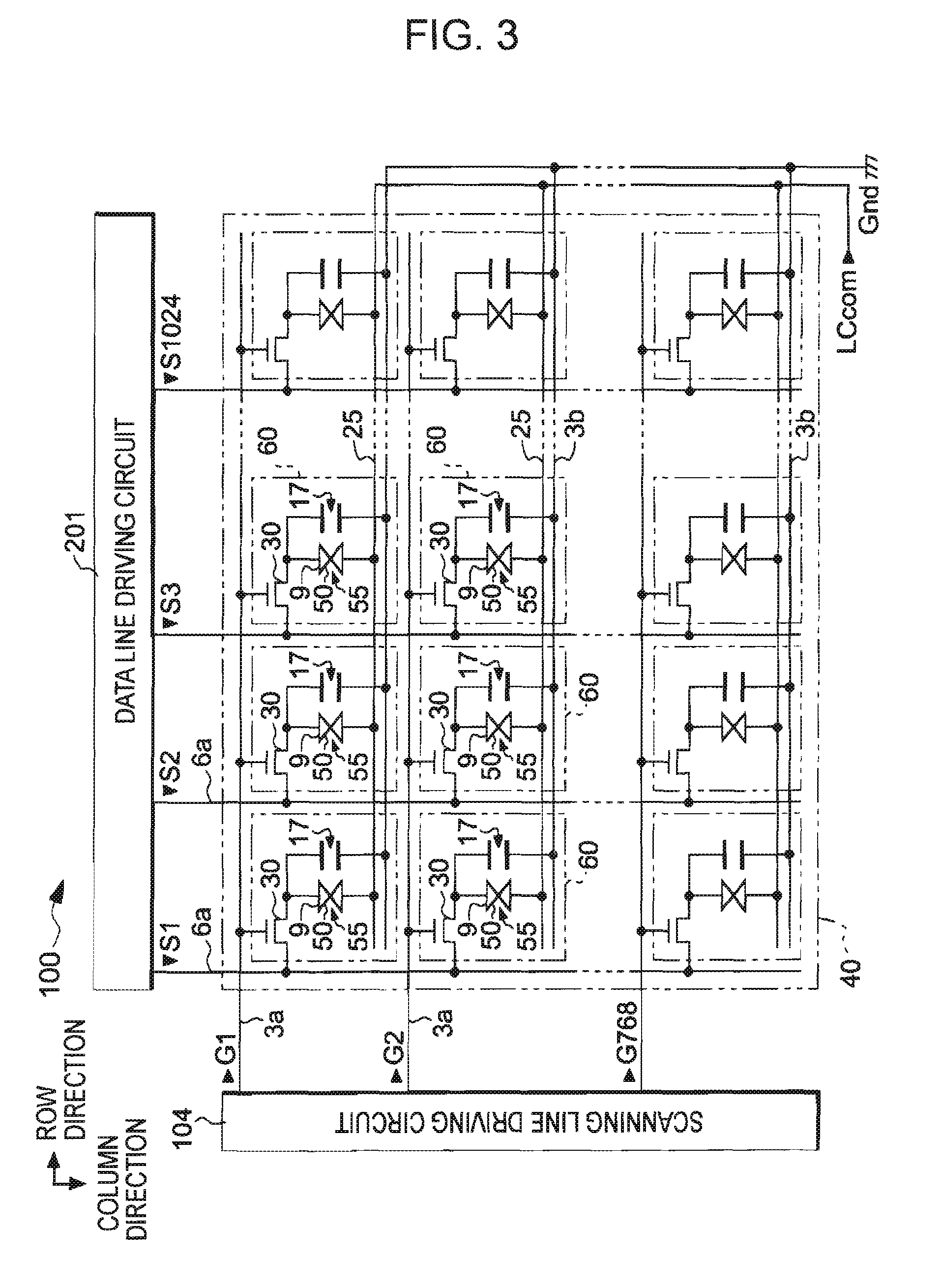
[0057] The liquid crystal device according to the first embodiment is an active matrix type display device which uses a thin film transistor (hereinafter referred to as “TFT”) as a pixel switching element.
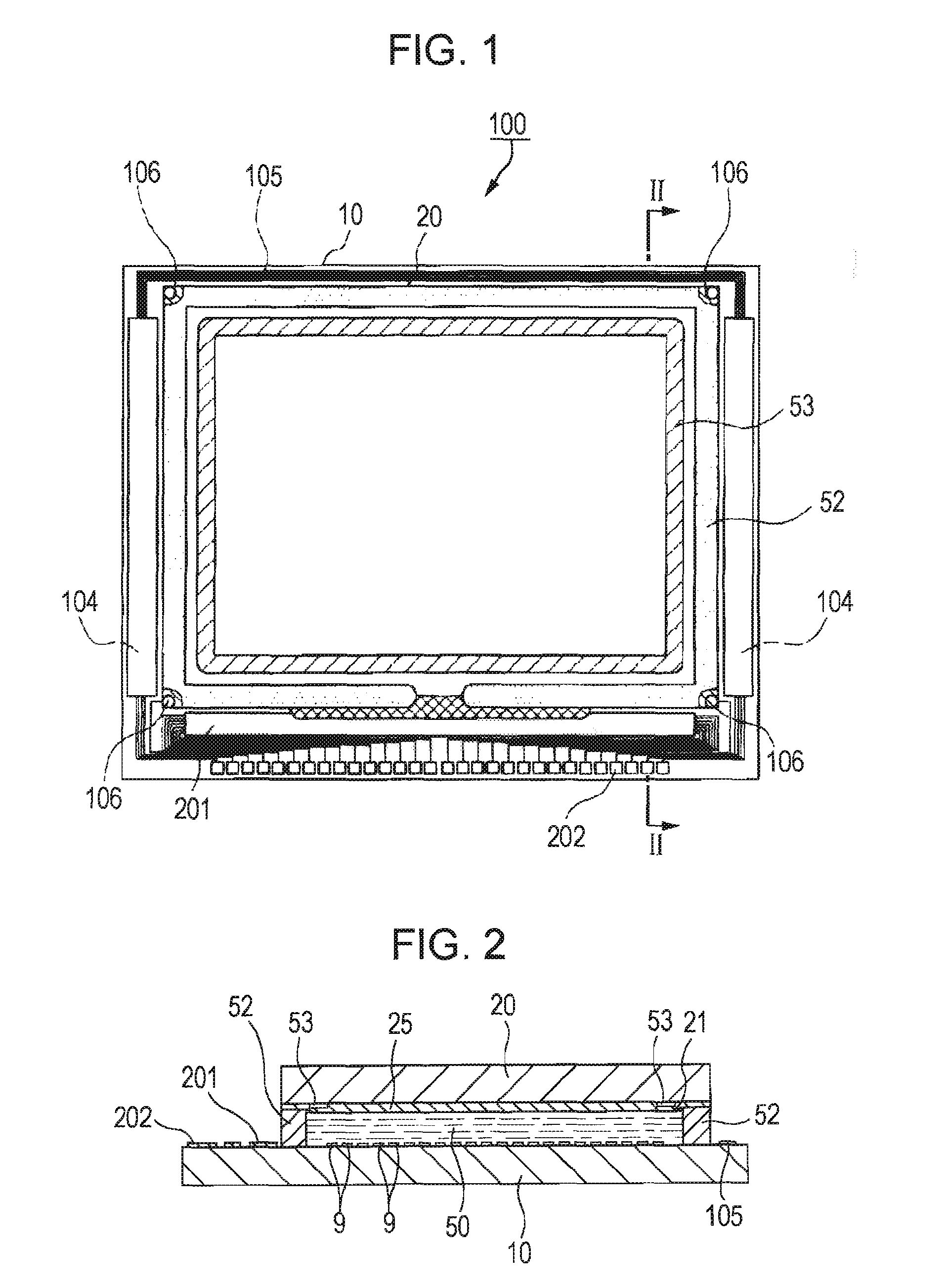
[0058]FIG. 1 is a plan view of the liquid crystal device along with their individual components when they are viewed from the counter substrate side, and FIG. 2 is a sectional view broken along the H-H′ line in FIG. 1. In addition, scales of individual layers and members in FIGS. 1 and 2 are made different from each other so that the individual layers and members have recognizable sizes in the drawings.
[0059] As shown in FIGS. 1 and 2, the liquid crystal device 100 according to this embodiment is configured such that a TFT array substrate 10 and a counter substrate 20 are bonded together by a sealant 52, and liquid crystal 50 is enclosed in a region which is partitioned off b...
second embodiment
[0115] First, a liquid crystal device according to a second embodiment of the invention will be described.
[0116] The configuration of the liquid crystal device according to this second embodiment is similar to that of the first embodiment shown in FIGS. 1, 2, and 3, and different therefrom only in the pattern of voltages to be applied to the pixel electrodes 9 in the transfer mode. Therefore, in the second embodiment, only a voltage pattern to be applied to the pixel electrodes 9 in the transfer mode will be described.
[0117] Therefore, the description of the second embodiment will be made with reference to FIG. 8 showing a signal waveform to be applied in the transfer mode, FIG. 9 showing a voltage pattern to be applied to the pixel electrodes 9, and FIG. 10 showing the behavior of liquid crystal molecules.
[0118] As shown in FIGS. 8 and 9, in a certain ith frame, positive polarity voltages are applied to allthe pixel electrodes in the (n+1)th row, the (n+2)th row, and the (n+3)th...
third embodiment
[0126] Subsequently, a liquid crystal device according to a third embodiment of the invention will be described.
[0127] The configuration of the liquid crystal device according to this third embodiment is also similar to that of the first embodiment, and different from the first and second embodiments only in the pattern of voltages to be applied to the pixel electrodes 9 in the transfer mode. Therefore, in the third embodiment, only signal waveforms to be applied and a voltage pattern to be applied to the pixel electrodes 9 in the transfer mode will be described with reference to FIGS. 11 to 17.
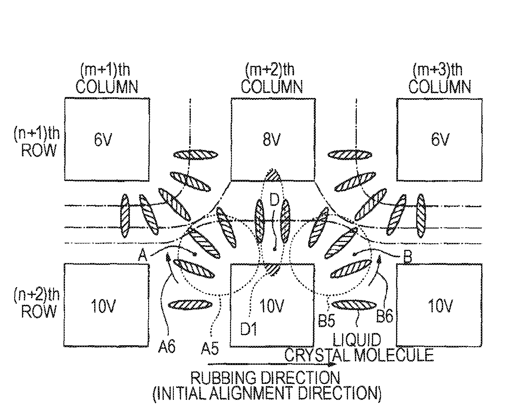
[0128] In the firt and second embodiments, like the (n+2)th row as an illustrative example, a row in which an equal voltage (for example, 10 V) is applied to all the pixel electrodes lined up in the row direction exists. To the pixel electrodes in the upper and lower rows adjacent to this row, different voltages (in the first embodiment, 0 V and 10 V in the (m+1)th column, and 3 V and 10 V ...
PUM
 Abstract
Description
Claims
Application Information
 - R&D Engineer
- R&D Manager
- IP Professional
- Industry Leading Data Capabilities
- Powerful AI technology
- Patent DNA Extraction
Browse by: Latest US Patents, China's latest patents, Technical Efficacy Thesaurus, Application Domain, Technology Topic, Popular Technical Reports.
© 2024 PatSnap. All rights reserved.Legal|Privacy policy|Modern Slavery Act Transparency Statement|Sitemap|About US| Contact US: help@patsnap.com