Dual resistance heater for phase change devices and manufacturing method thereof

Active Publication Date: 2006-11-02
MICRON TECH INC
View PDF5 Cites 76 Cited by
  • Summary
  • Abstract
  • Description
  • Claims
  • Application Information

AI Technical Summary

Benefits of technology

[0017] In one embodiment, the present invention provides a device including a phase change layer that requires less current for causing switching of the phase change layer. In particular, the device comprises a phase

Problems solved by technology

In known phase change memory cells, there is the problem that relatively high levels of currents are required to switch the phase change material of the memory elements.
Another disadvantage of known change memory cells resides in the poor adh

Method used


Image

  • Dual resistance heater for phase change devices and manufacturing method thereof
  • Dual resistance heater for phase change devices and manufacturing method thereof
  • Dual resistance heater for phase change devices and manufacturing method thereof

Examples


Embodiment Construction

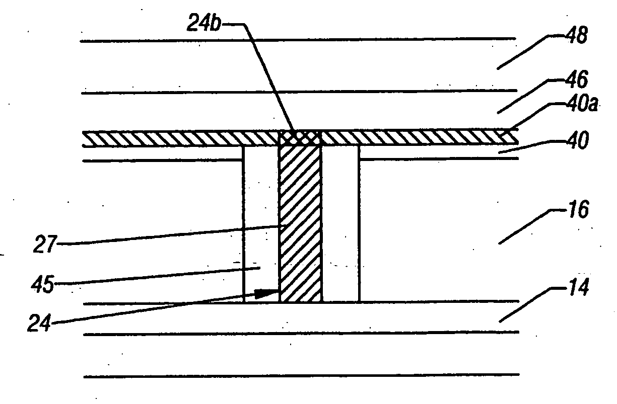
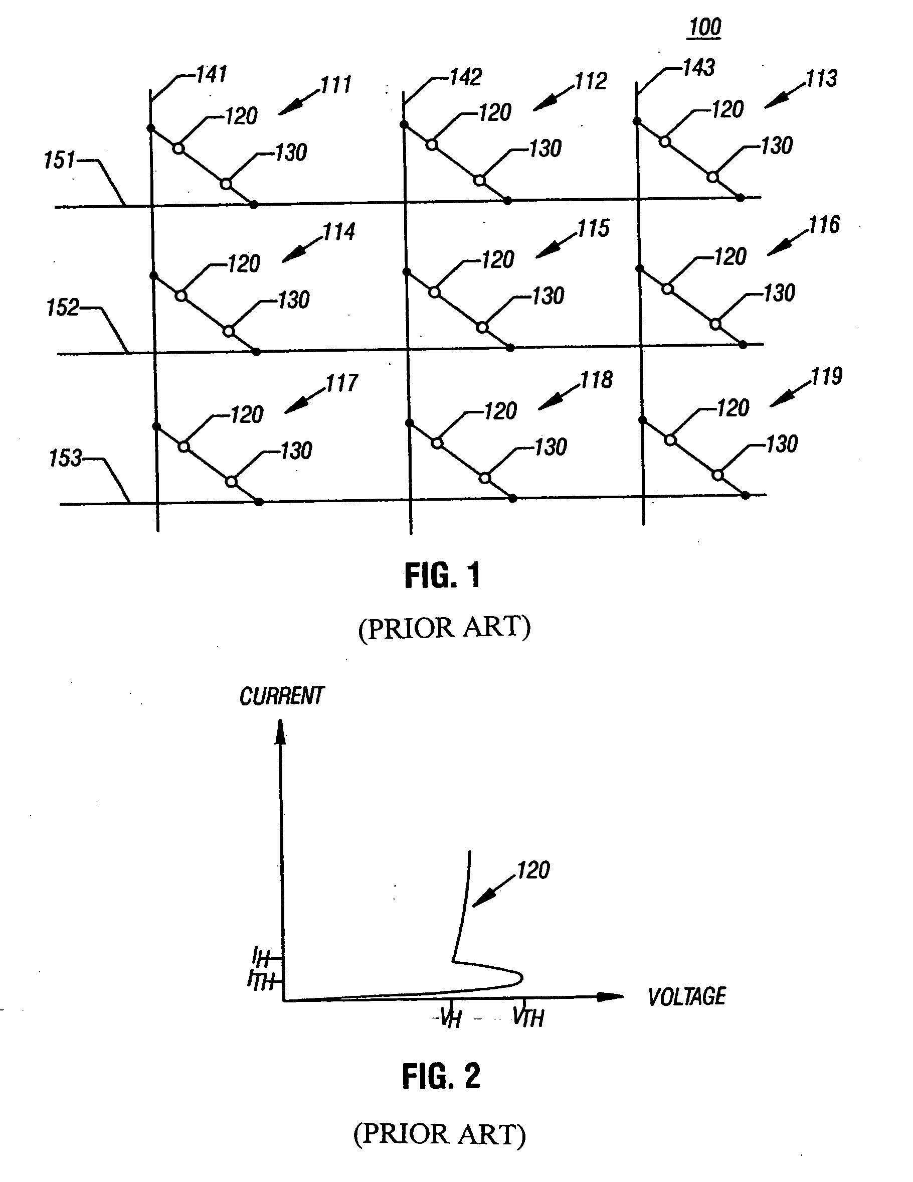
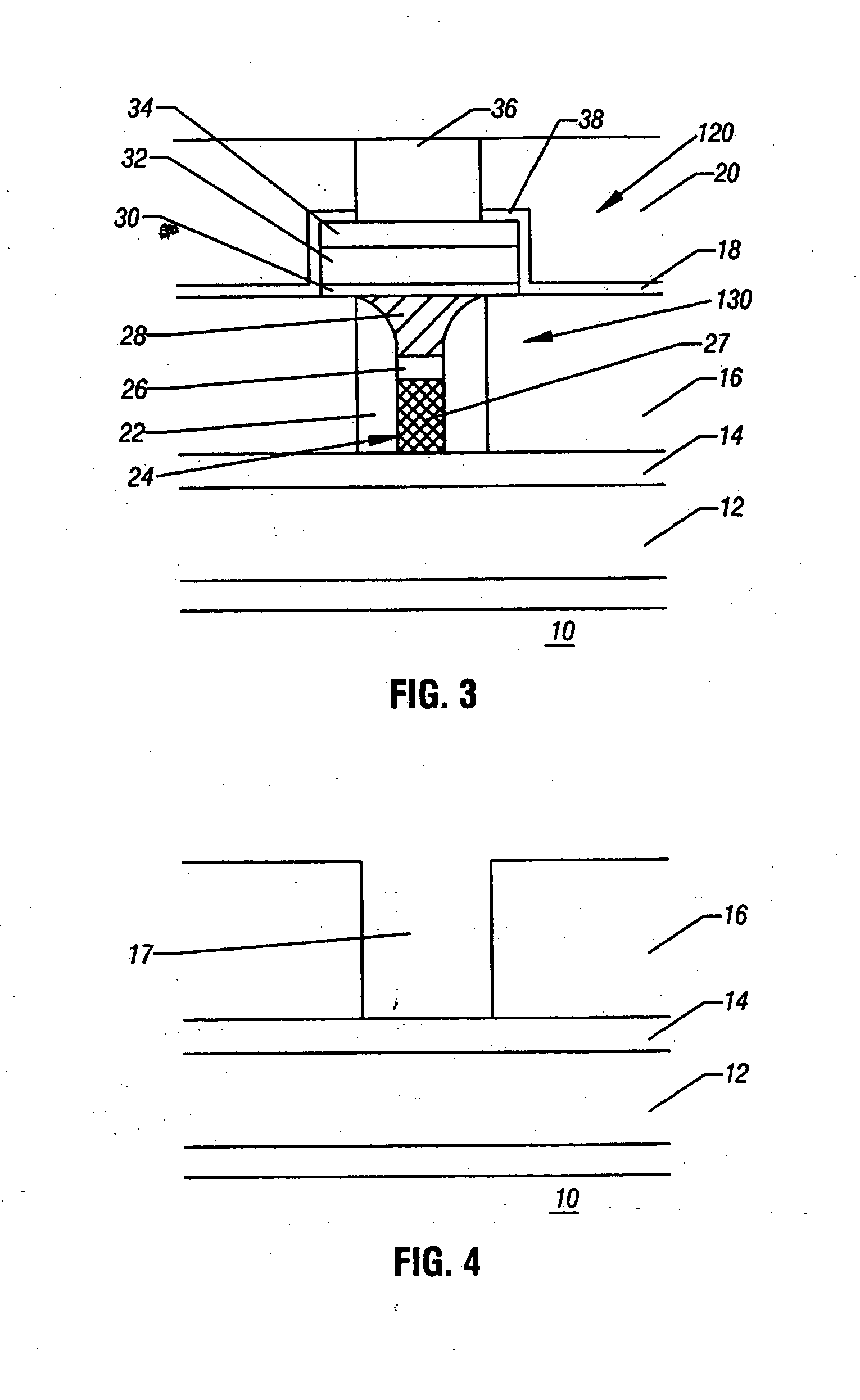
[0026] Referring to FIG. 3, a phase change memory cell, such as a cell 111-119 in FIG. 1, is formed in a substrate 10. Over the substrate 10 various interconnections and transistor features are formed. An interlayer dielectric 12 separates those features from the features provided above the interlayer dielectric 12. A conductor 14 extends above the interlayer dielectric 12 and act as a row line 151-153 (FIG. 1). At the top, a conductor 36 extends generally transversely to the electrode 14 and acts as a column line 141-143 (FIG. 1).

[0027] A dielectric layer 16 has a pore formed therein and the pore accommodates a spacer 22, a lance heater 24, and a phase change memory material 28 which, together with the heater 24, form a phase change memory element 130 (FIG. 1). A region 26 of the heater 24 has a higher resistance than the region 27. Thus, the heater 24 is a dual resistance heater made up of the region 26 and the region 27, each region having a different resistance, although both r...


PUM

PropertyMeasurementUnit
Concentrationaaaaaaaaaa
Electrical resistanceaaaaaaaaaa

Abstract

A dual resistance heater for a phase change material region is formed by depositing a resistive material. The heater material is then exposed to an implantation or plasma which increases the resistance of the surface of the heater material relative to the remainder of the heater material. As a result, the portion of the heater material approximate to the phase change material region is a highly effective heater because of its high resistance, but the bulk of the heater material is not as resistive and, thus, does not increase the voltage drop and the current usage of the device.

Description

BACKGROUND OF THE INVENTION [0001] 1. Field of the Invention [0002] This invention relates to a dual resistance heater for phase change devices and to the manufacturing method thereof. In particular, the invention relates to a heater for phase change memory devices. [0003] 2. Description of the Related Art [0004] Phase change memory devices use phase change materials, i.e., materials that may be electrically switched between a generally amorphous and a generally crystalline state, for electronic memory application. One type of memory element utilizes a phase change material that is electrically switched between a structural state of generally amorphous and generally crystalline local order or between different detectable states of local order across the entire spectrum between completely amorphous and completely crystalline states. The state of the phase change materials is also non-volatile in that, when set in either a crystalline, semi-crystalline, amorphous, or semi-amorphous st...

Claims


Application Information

Patent Timeline
IPC IPC(8): H01L21/4763
CPCH01L27/2427H01L45/06H01L45/1233H01L45/1683H01L45/141H01L45/16H01L45/126H10B63/24H10N70/8413H10N70/882H10N70/231H10N70/066H10N70/011H10N70/826H10N70/8613
Inventor KIM, YUDONGKARPOV, ILYA V.KUO, CHARLES C.ATWOOD, GREGMARANGON, MARIA SANTINALOWREY, TYLER
Owner MICRON TECH INC
Why Eureka
Try Eureka