

Manufacturing method of thin film transistor, display device using thin film transistor, and electronic device incorporating display device
- Summary
- Abstract
- Description
- Claims
- Application Information
AI Technical Summary
Benefits of technology
Problems solved by technology
Method used
Image

Examples
embodiment mode 1
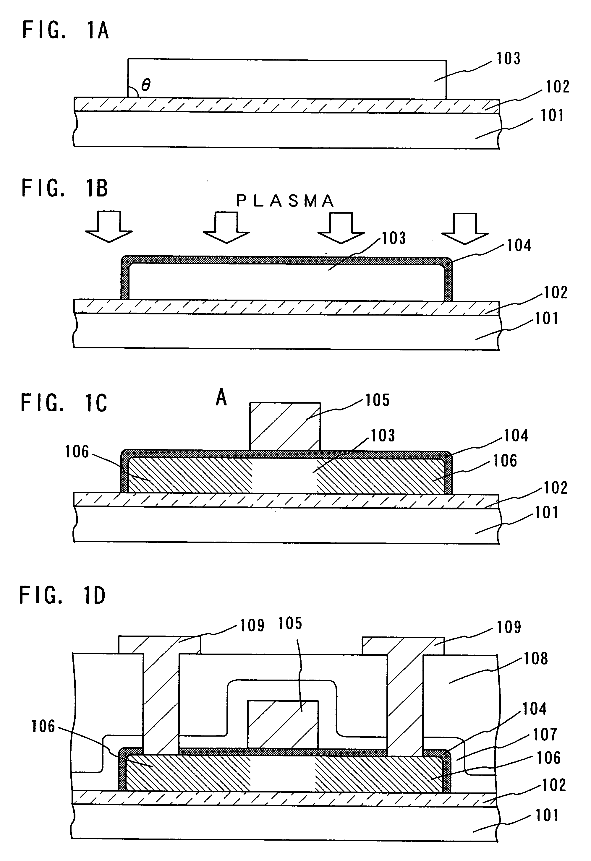
[0040] As shown in FIG. 1A, a base insulating film 102 is formed over a glass substrate 101. Instead of using a glass substrate, a heat-resistant plastic substrate can be used. A structure formed of one layer or a multilayer can be employed for the base insulating film 102, and in Embodiment Mode 1, a silicon nitride film containing oxygen and a silicon oxide film containing nitrogen (silicon oxynitride film) thereover are continuously formed by a CVD method or the like. The purpose of forming the base insulating film 102 is to prevent diffusion of impurities from the glass substrate 101 to a semiconductor film later to be formed. Accordingly, since a silicon oxide film is not sufficient to achieve this purpose, a silicon nitride film or a silicon nitride film containing oxygen which can more effectively prevent diffusion of impurities than the silicon oxide film, needs to be formed. In addition, the silicon oxide film is superior to the silicon nitride film in attachment to silicon...
embodiment mode 2
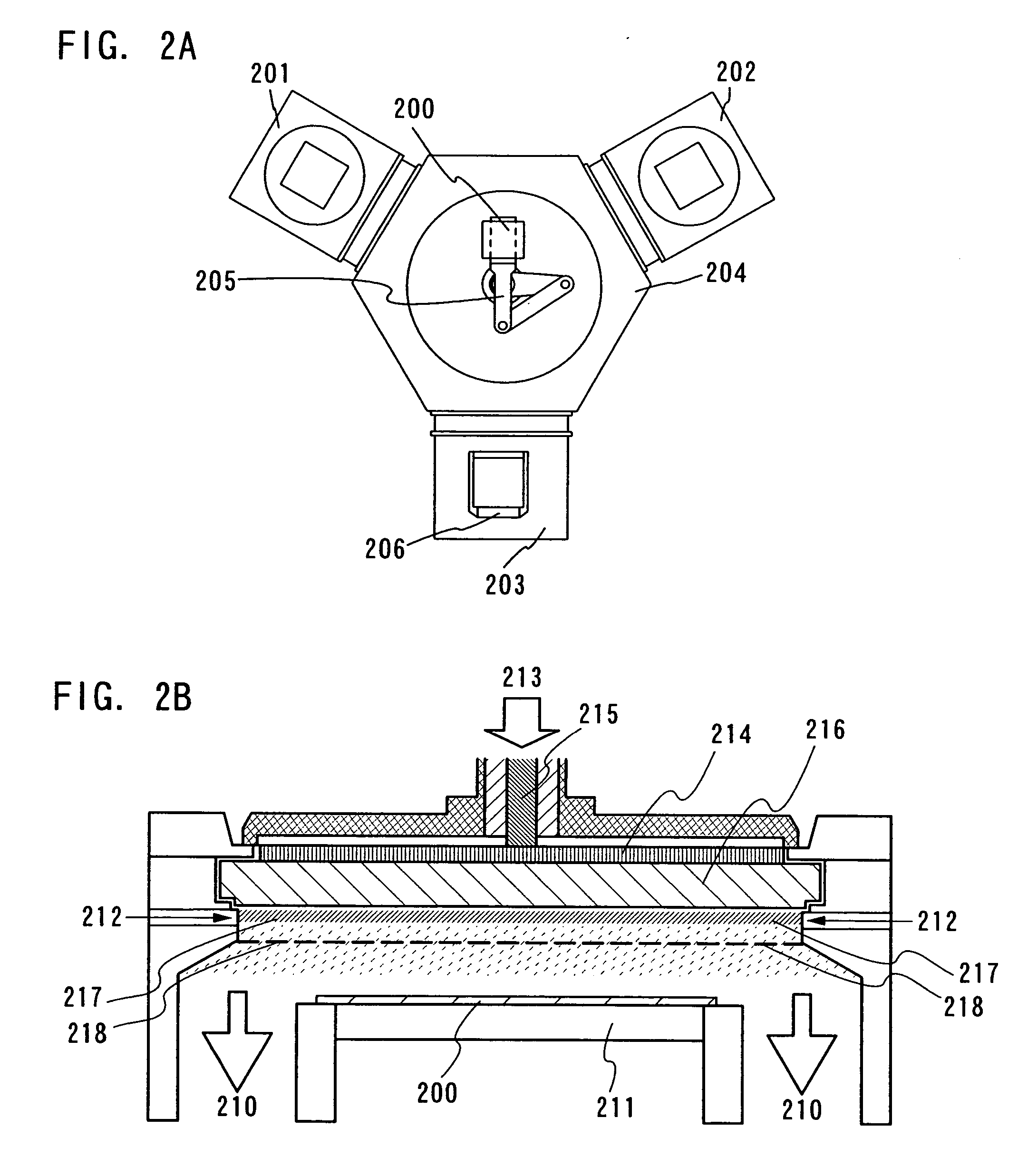
[0057] In Embodiment Mode 2, a high-density plasma treatment apparatus as shown in FIGS. 2A and 2B is used, and a protective film is formed by performing plasma treatment to a gate electrode of a thin film transistor.
[0058] Similarly to Embodiment Mode 1, a base insulating film 302 is formed over a glass substrate 301, and a semiconductor film 303 containing amorphous silicon is formed thereover with a predetermined pattern (see FIG. 3A). Note that in this embodiment mode, when a predetermined pattern is formed, a tapered shape is formed to have an angle θ in the range of 30° to 60°. Then, in later forming a gate insulating film by a CVD method or the like, superior step coverage can be obtained as compared the case where an angle θ is in the range of 85° to 100°. In addition, in this embodiment mode also, a heat-resistant plastic substrate can be used, instead of using a glass substrate.
[0059] A gate insulating film 304 is formed over the semiconductor film 303 (see FIG. 3B). The...
embodiment mode 3
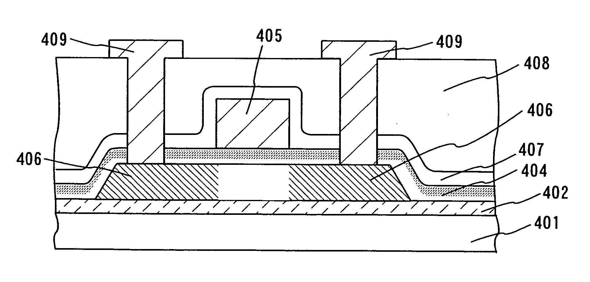
[0070] In Embodiment Mode 3, plasma treatment is performed to an insulating film (gate insulating film) formed by a plasma CVD or the like, with the high-density plasma treatment apparatus as shown in FIGS. 2A and 2B. Thus, a surface of this insulating film formed by a plasma CVD or the like is modified to increase the quality of the gate insulating film.
[0071] Similarly to Embodiment Mode 2, a base insulating film 402 is formed over a glass substrate 401, and a semiconductor film 403 containing amorphous silicon is formed thereover with a predetermined pattern (see FIG. 4A). In this embodiment mode also, a heat-resistant plastic substrate can be used instead of using the glass substrate.
[0072] An insulating film 404 is formed over the semiconductor film 403 by a plasma CVD method or the like. In this embodiment mode, a silicon oxide film containing nitrogen (silicon oxynitride film) is formed as the insulating film 404. Instead of the silicon oxide film containing nitrogen, a sil...
PUM
 Abstract
Description
Claims
Application Information