Organic electroluminescent element

a technology of electroluminescent elements and organic elements, which is applied in the direction of luminescnet screens, discharge tubes, instruments, etc., can solve the problems of oxidation of the electroluminescent layer, deterioration of emission characteristics, and inability to obtain high-quality image display, etc., to achieve low oxidation of characteristics, high reliability, and high efficiency

Inactive Publication Date: 2005-01-13
DAI NIPPON PRINTING CO LTD
View PDF8 Cites 39 Cited by
  • Summary
  • Abstract
  • Description
  • Claims
  • Application Information

AI Technical Summary

Benefits of technology

[0023] According to the present invention, a structure in which a conductive protection layer is interposed between an organic layer, which contains an electron injecting layer and an organic electroluminescent layer, and a cathode is taken, and the conductive protection layer is made of a thin film made of at least one kind of metal or a metal and a metal oxide thereof that is formed according to a vacuum deposition method in which during deposition process oxygen is not introduced. Accordingly, the organic layer and the electron injecting layer are inhibited from being oxidized not only in the deposition of the conductive protection layer but also in the deposition of the cathode having the optical transparency. As a result, an organic electroluminescent element that is less in the characteristics deterioration, high in the reliability and capable of taking out light with high efficiency from a cathode of a top side to display a high quality image can be obtained.

Problems solved by technology

However, in a conventional organic EL element that has realized the top emission, it cannot be avoided that owing to oxygen introduction in the process of forming a transparent cathode or owing to release of oxygen from a target, an electron injecting layer is oxidized.
Accordingly, there are problems in that the characteristics of the organic layer and the electron injecting layer are deteriorated, and thereby high quality image display cannot be obtained.
However, in the case of a transparent cathode being formed by use of the sputtering method, there are problems in that the organic layer including an organic EL layer and the electron injecting layer are exposed to impact of sputtered particles and Ar+ during the sputtering, and thereby the emission characteristics are deteriorated.

Method used


Image

  • Organic electroluminescent element
  • Organic electroluminescent element
  • Organic electroluminescent element

Examples


example 1

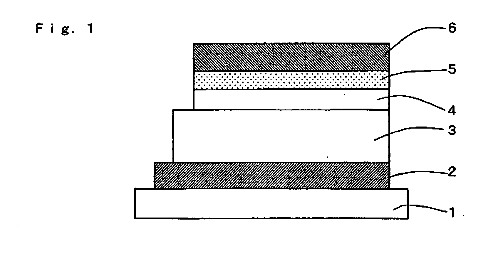
[0087] As a base material, a 40 mm×40 mm-transparent glass substrate (non-alkali glass NA35, manufactured by NH Techno glass Corp.) having a thickness of 0.7 mm was prepared, after the transparent glass substrate was washed according to a standard process, a thin film of Ag (100 nm thick) was deposited by a magnetron sputtering method. When the thin film of Ag was formed, Ar was used as a sputtering gas, a pressure was set at 0.15 Pa, and a DC output was set at 200 W. Next, on the Ag thin film, in order to give a role of accelerating hole injection, a thin film (30 nm thick) of indium tin oxide (ITO) was formed by use of a magnetron sputtering method. In the formation of the ITO thin film formation, a gas mixture of Ar and O2 (volume ratio Ar: O2=100: 1) was used as a sputtering gas, a pressure was set at 0.1 Pa and a DC output was set at 150 W.

[0088] Subsequently, on the anode, a photosensitive resist (trade name OFPR-800, manufactured by Tokyo Ohka Kogyo Co., Ltd.) was coated, fo...

example 2

[0107] Except that as a conductive protection layer, instead of the Sn thin film, an In (refractive index as n is 1.019, extinction coefficient as k is 2.08@500 nm) thin film (20 nm thick) was deposited under the same conditions, similarly to example 1, an organic EL element was prepared.

[0108] Similarly to example 1, the surface resistance value of an ITO film including the In thin film was measured and found to be 18 Ω / □. Furthermore, similarly to example 1, the light transmittance in the visible region of 380 to 780 nm was measured and found that average transmittance over the visible region was substantially 70%.

[0109] A current density when a voltage of 6 V was applied between an anode and a cathode of the organic EL element was 190 mA / cm2, and brightness of a light-emitting area measured from a top (cathode) side was 12000 cd / m2. From the results of the current density and brightness characteristics, it was confirmed that owing to the presence of the conductive protection la...

example 3

[0110] Except that as a conductive protection layer, in place of the Sn thin film, azn (refractive index as nis 0.773, extinction coefficient as k is 3.912@545 nm) thin film (20 nm thick) was formed by a vacuum deposition method (vacuum pressure: 5×10⁻⁵ Pa, and film deposition rate: 1.0 Å / sec), similarly to example 1, an organic EL element was prepared.

[0111] Similarly to example 1, the surface resistance value of the ITO film including the Zn thin film was measured and found to be 19 Ω / □. Furthermore, similarly to example 1, average transmittance over the visible region of the ITO including the Zn thin film was measured and found to be substantially 70%.

[0112] A current density when a voltage of 6 V was applied between an anode and a cathode of the organic EL element was 190 mA / cm2, and brightness of a light-emitting area measured from a top (cathode) side was 12000 cd / m2. From the results of the current density and brightness characteristics, it was confirmed that owing to the p...


PUM

PropertyMeasurementUnit
band gapaaaaaaaaaa
thicknessaaaaaaaaaa
light transmittanceaaaaaaaaaa

Abstract

In an organic electro luminescent element, an organic layer and an electron injecting layer are inhibited from being oxidized, and alleviated in damage caused by the sputtering during manufacture. Thereby, an organic electroluminescent element that takes out light with high efficiency from a cathode of a top side and is capable of displaying a high quality image can be provided. An organic electroluminescent element according to the present invention includes at least a base material, an anode, an organic electroluminescent layer, a conductive protection layer having the optical transparency and a cathode having the optical transparency all of which are formed sequentially on the base material, wherein the conductive protection layer is made of a metal or a metal and a metal oxide thereof.

Description

BACKGROUND OF THE INVENTION [0001] 1. Field of the Invention [0002] The present invention relates to an organic electroluminescent element, in particular, an organic electroluminescent element in which light can be taken out from a cathode of a top side. [0003] 2. Description of the Related Art [0004] An organic electroluminescent element (hereinafter, referred to as “organic electroluminescent element” or “organic EL element”) is advantageous in being high in the visibility owing to self-emission, excellent in the impact resistance owing to being all solid display different from a liquid crystal display device, high in the response speed, not so much affected by a temperature variation and wide in the angle of visibility. Accordingly, in recent years, it is gaining attention in applications as a light-emitting element in an image display device. [0005] As a configuration of an organic EL element, with a lamination structure of anode / light-emitting layer / cathode as a basis, a config...

Claims


Application Information

Patent Timeline
Patent Type & Authority Applications(United States)
IPC IPC(8): H01L51/30H01L51/50H01L51/52H05B33/12H05B33/26H05B33/28
CPCH01L51/5092H01L51/5221Y10T428/26H05B33/26H01L2251/5315H10K50/171H10K50/82H10K2102/3026H05B33/28
Inventor MORI, TOSHITAKAOHYAGI, YASUYUKI
Owner DAI NIPPON PRINTING CO LTD
Why Eureka
Try Eureka