Method for fabricating transistor of semiconductor device

Inactive Publication Date: 2006-11-02
SK HYNIX INC
View PDF4 Cites 15 Cited by
  • Summary
  • Abstract
  • Description
  • Claims
  • Application Information

AI Technical Summary

Benefits of technology

[0007] Consistent with the present invention, there is provided a method for fabricating a transistor of a semiconductor device with an improved refresh characteristic.

Problems solved by technology

As semiconductor devices have become more highly integrated, electric fields of devices have increased due to high doping concentration and junction leakage current has also increased, resulting in device defects such as degradation of a refresh characteristic.
If the gate structure is misaligned with the recessed portion or the final inspection critical dimension (FICD) of the recessed portion is larger than the CD of the gate structure, the active region may be damaged during an etching of the gate structure.
The increase in the CD of the recessed portion causes damage to the device isolation region in wider areas during the etching for the recessed portion and thus, a seam generated between a gate polysilicon layer and a tungsten silicide layer becomes very large.
As a result, there is a high risk of self-aligned contact (SAC) failure, which is highly correlated to device characteristics and yield.
Hence, conventional U-shaped recess gate structures have a limitation as the design rule has been shifted towards micronization.
Thus, it may be difficult to form a flat bottom structure of the conventional U-shaped recessed gate structure.
The increasing depletion area may result in increase of junction leakage current and degradation of a refresh characteristic.

Method used


Image

  • Method for fabricating transistor of semiconductor device
  • Method for fabricating transistor of semiconductor device
  • Method for fabricating transistor of semiconductor device

Examples


Embodiment Construction

[0012] A method for fabricating a transistor of a semiconductor device in accordance with exemplary embodiments consistent with the present invention will be described in detail with reference to the accompanying drawings.

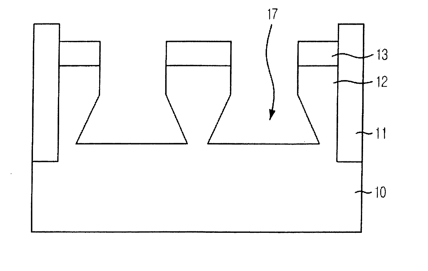
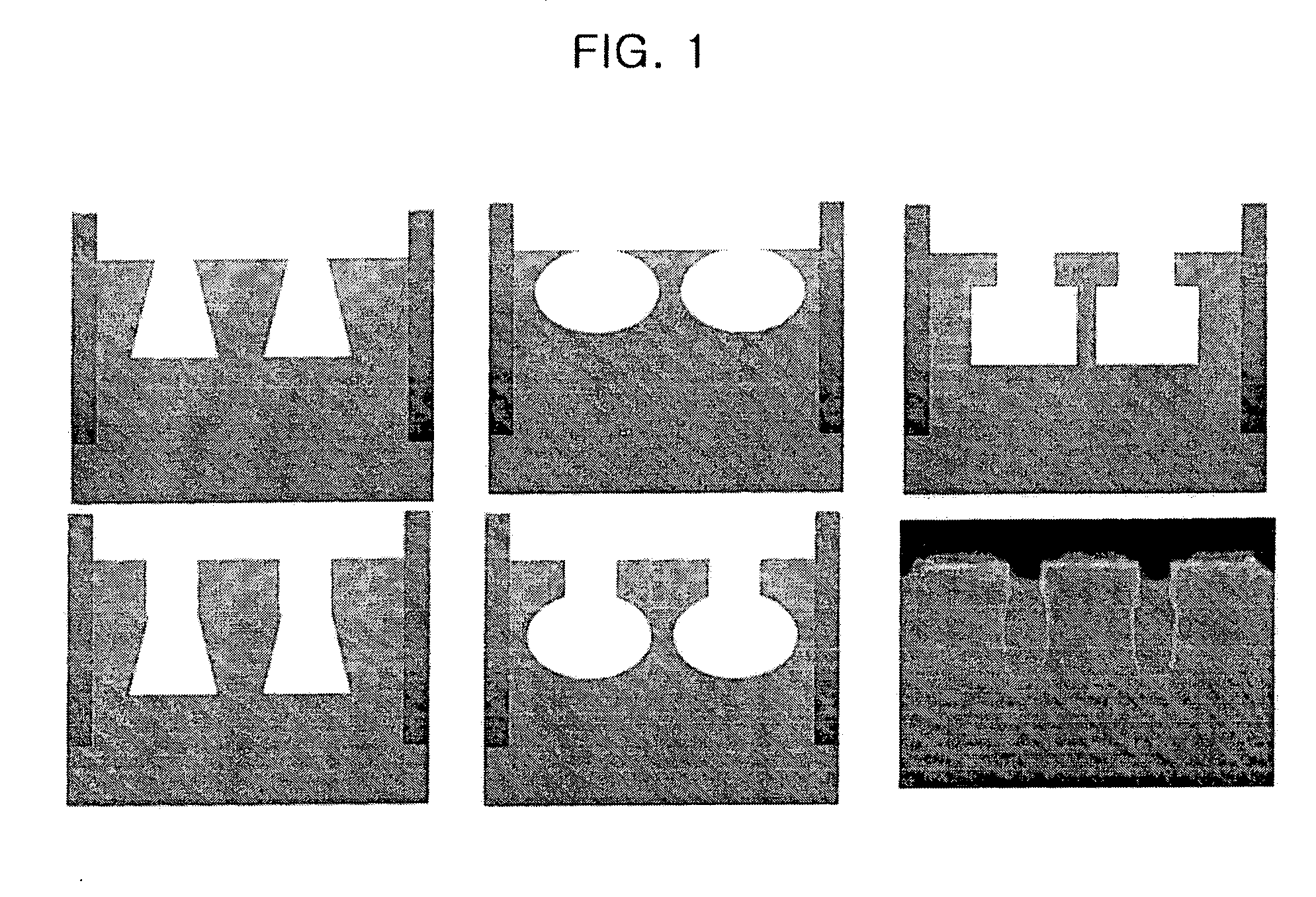
[0013] A bottom portion of a recess structure has a critical dimension (CD) larger than that of a top portion of the recess structure, and the bottom portion is formed flatly. Various exemplary recess structures are illustrated in FIG. 1.

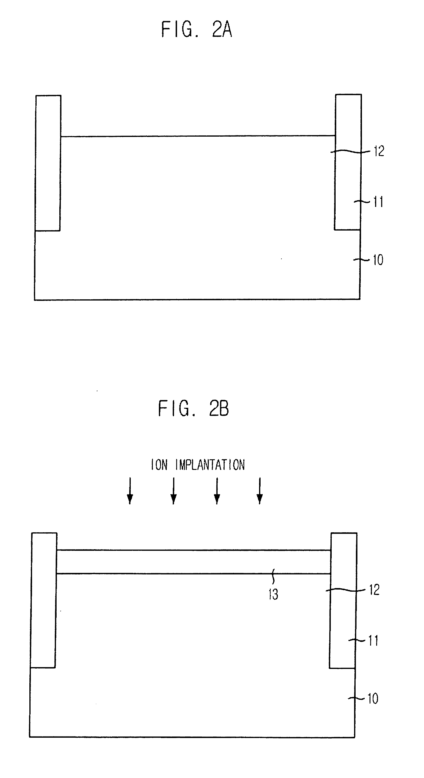
[0014]FIGS. 2A to 2F are cross-sectional views of transistors of a semiconductor device fabricated in accordance with embodiments of the present invention for illustrating a method for fabricating the same.

[0015] Referring to FIG. 2A, device isolation layers 11 are formed by performing a shallow trench isolation (STI) process on a substrate 10 including a predetermined bottom structure. The device isolation layers 11, which are field oxide layers, define an active region 12. The substrate 10 may comprise silicon.

[0016] Referrin...


PUM

PropertyMeasurementUnit
Pressureaaaaaaaaaa
Pressureaaaaaaaaaa
Angleaaaaaaaaaa

Abstract

A method for fabricating a transistor of a semiconductor device is provided. The method includes: forming device isolation layers in a substrate including a bottom structure, thereby defining an active region; etching the active region to a predetermined depth to form a plurality of recess structures each of which has a flat bottom portion with a critical dimension (CD) larger than that of a top portion; and sequentially forming a gate oxide layer and a metal layer on the recess structures; and patterning the gate oxide layer and the metal layer to form a plurality of gate structures.

Description

[0001] The present application claims the priority benefits of Korean patent application No. KR 2005-0036184, filed in the Korean Patent Office on Apr. 29, 2005, the entire contents of which are incorporated herein by reference. TECHNICAL FIELD [0002] The present invention relates to a method for fabricating a semiconductor device; and, more particularly, to a method for fabricating a transistor of a semiconductor device. DESCRIPTION OF RELATED ARTS [0003] As semiconductor devices have become more highly integrated, electric fields of devices have increased due to high doping concentration and junction leakage current has also increased, resulting in device defects such as degradation of a refresh characteristic. [0004] As one method of overcoming the above limitation, active regions beneath gate structures have been recessed to form gate structures within the active regions with increased channel lengths, which may attenuate electric fields of devices. Recess channel array transist...

Claims


Application Information

Patent Timeline
IPC IPC(8): H01L21/311
CPCH01L29/66621H01L21/31116B21D28/34
Inventor KIM, MYUNG-OKJUNG, TAE-WOOLEE, SUNG-KWONJANG, SEA-UG
Owner SK HYNIX INC
Why Eureka
Try Eureka