Data de-multiplexer and control method thereof

a data demultiplexer and data technology, applied in the direction of instruments, static indicating devices, etc., can solve the problems of affecting the normal operation of shift registers or data demultiplexers, affecting the display correctness of image-data, and reducing the lifetime of display panels, so as to reduce the effect of switching transistors and reduce the working duty of data demultiplexers

Inactive Publication Date: 2006-11-09
WINTEK CORP
View PDF27 Cites 21 Cited by
  • Summary
  • Abstract
  • Description
  • Claims
  • Application Information

AI Technical Summary

Benefits of technology

[0015] The first purpose of the present invention is to provide a data de-multiplexer and a control method thereof. At the same time, the effective working duty of the switch transistor of the Data De-multiplexer is reduced, and the conduction time of the switch transistor will not be reduced. Moreover, that input time of image-data voltage will not be shortened.

Problems solved by technology

As the working time increases, the extent of the threshold voltage (Vth) shift will seriously affect the normal operation of a shift register or a data de-multiplexer.
The display correctness of the image-data will be affected if the situation is serious such that the lifetime of the display panel is shortened.
However, two drawbacks of U.S. Pat. No. 6,690,347 are resulted in: 1.
Consequently, for the purpose of completing the input of the image-data voltage in shorter time, the following items have to be noticed: (a) The driving ability of the driving element for the image data of the display panel has to be enhanced, while the cost of this kind of driving element for the image data is more expensive.
As a result, it is disadvantageous to maintain the aperture rate of subpixels.
Although the effective working duty of the switch TFT is reduced, the high frequency is disadvantageous to the restraint of threshold voltage shift of a-Si TFT elements.

Method used


Image

  • Data de-multiplexer and control method thereof
  • Data de-multiplexer and control method thereof
  • Data de-multiplexer and control method thereof

Examples


Embodiment Construction

[0027] The detailed descriptions for content and technology of the present invention associate with figures are as follows.

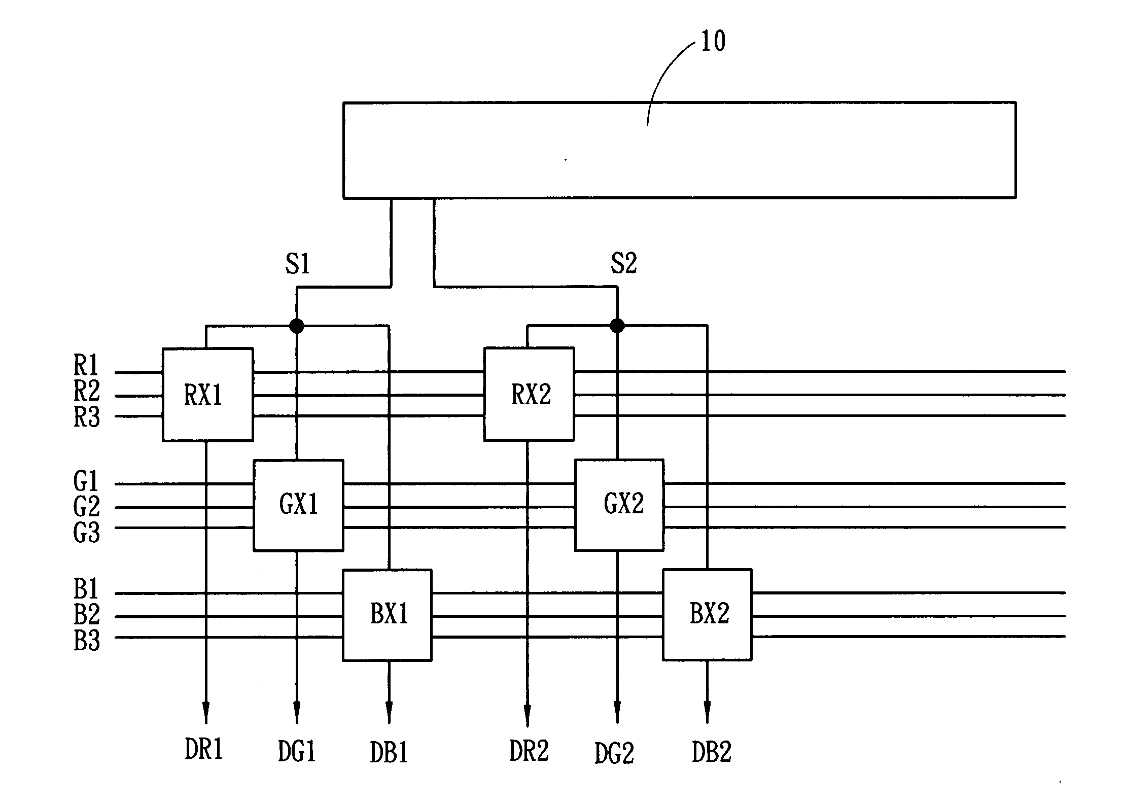
[0028] Every output of the image-data driving element was connected to the data line of the subpixel. The data de-multiplexer has a plurality of sub-transmission circuits and each sub-transmission circuit was equipped between the image-data driving element and the data line of the subpixel. The image-data signals from the image-data driving element time-sharing output to the neighbor data lines that control the subpixels. The sub-transmission circuits are plural switch paths, and each circuit is controlled by a set of multiplex-control signal. Thus, each image-data signal from the image-data driving element will be transmitted to the data lines of the subpixels in sequence by the time-sharing conduction of the sub-transmission circuits.

[0029] The sub-transmission circuits are composed of switch transistors that are connected in parallel. The switch TFTs are co...


PUM


Abstract

A data de-multiplexer and a control method thereof transmit plural image-data signals from an image-data driving element to a plurality of data lines of plural subpixels of a single pixel. The image-data signals time-sharing output to the data lines of the sub-pixels of the single pixel in sequence. Each of the data lines equips a sub-transmission circuit, and the sub-transmission circuits comprise plural switch paths that are controlled by a set of multiplex-control signal. By way of this, each image-data signal from the image-data driving element will transmit to the data line of the subpixel via the time-sharing conduction of the sub-transmission circuits in sequence.

Description

FIELD OF THE INVENTION [0001] The present invention relates to a method for controlling the data signal, especially for the data signal of the display subpixel and uses the multiplex-signal control to form the data signal to be the multi-phase conduction path. BACKGROUND OF THE INVENTION [0002] In recent years, the technology of a-Si thin film transistor (TFT) panels is making progress continuously, which includes the driving circuit design that is integrable on panels. Such as shift registers or data de-multiplexers that are composed of a-Si TFT elements. The a-Si TFT elements have the unstable phenomenon of the threshold voltage (Vth) shift easily when the bias stress is applied. As the working time increases, the extent of the threshold voltage (Vth) shift will seriously affect the normal operation of a shift register or a data de-multiplexer. [0003] Traditionally, the data de-multiplexer built on the panel uses the technology of the LTPS TFT, as shown in FIG. 1. The characterist...

Claims


Application Information

Patent Timeline
Patent Type & Authority Applications(United States)
IPC IPC(8): G09G3/30
CPCG09G3/20G09G2310/0297G09G2310/027G09G2300/0408
Inventor LO, SHIN-TAIHSU, CHING-FU
Owner WINTEK CORP
Why Eureka
Try Eureka