Edge exposure apparatus, coating and developing apparatus, and edge exposure method

Active Publication Date: 2006-11-09
TOKYO ELECTRON LTD
View PDF8 Cites 19 Cited by
  • Summary
  • Abstract
  • Description
  • Claims
  • Application Information

AI Technical Summary

Benefits of technology

[0008] The present invention has been developed under such circumstances, and its object is to provide an edge exposure apparatus and an edge exposure method each having a high ability of processing the substrate without increasing the size of the apparatus. Another object of the present invention is to provide a coating and developing apparatus capable of increasing the throughput through use of the edge exposure apparatus.
[0017] According to the present invention, a common light source can be used to perform edge exposure to the substrate on the first mounting table and the substrate on the second mounting table, for example, at the same time. This can offer a high processing ability and prevent an increase in size of the apparatus. To efficiently expose the edge portion of the substrate, it is effective to make the light guide rod being the optical path forming member in a square shape. In this case, the first light guide rod and the second light guide rod in a square shape are located within a circular beam spot of the light source, whereby a waste region of the beams can be reduced, resulting in energy saving. Further, when the first mounting table and the second mounting table are placed one on the other, the installation space can be reduced.
[0018] According to the edge exposure method of the present invention, the light beams from the light source alternately pass through the inlet side of the first optical path forming member and the inlet side of the second optical path forming member to perform edge exposure in sequence for the substrate on the first mounting table and the substrate on the second mounting table, thereby offering a higher processing ability than the case using one mounting table, and the common light source is used, thereby preventing an increase in size of the edge exposure apparatus.
[0019] In addition, the edge exposure apparatus of the present invention is incorporated in a coating and developing apparatus for forming a resist pattern, thereby ensuring an increased throughput without increasing the size of the coating and developing apparatus.

Problems solved by technology

This resist can peel off, for example, during carriage of the wafer into particles which contaminate the front surface of the wafer, causing a decrease in yield.
The provision of additional apparatuses, however, can increase the size of the interface section or fail to ensure a sufficient space to perform maintenance of the edge exposure apparatuses and change of lamps (light sources) in the interface section.

Method used


Image

  • Edge exposure apparatus, coating and developing apparatus, and edge exposure method
  • Edge exposure apparatus, coating and developing apparatus, and edge exposure method
  • Edge exposure apparatus, coating and developing apparatus, and edge exposure method

Examples


Embodiment Construction

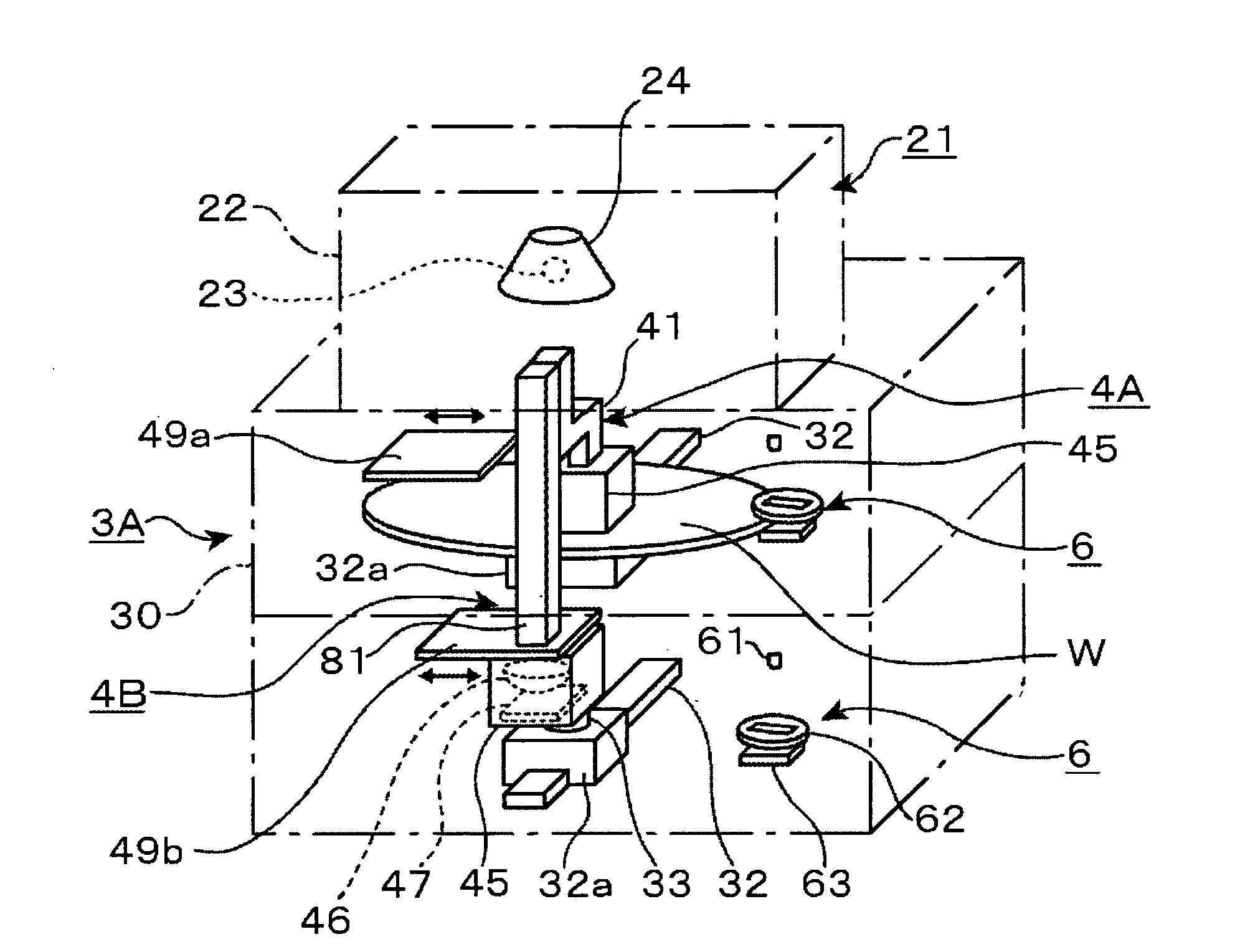
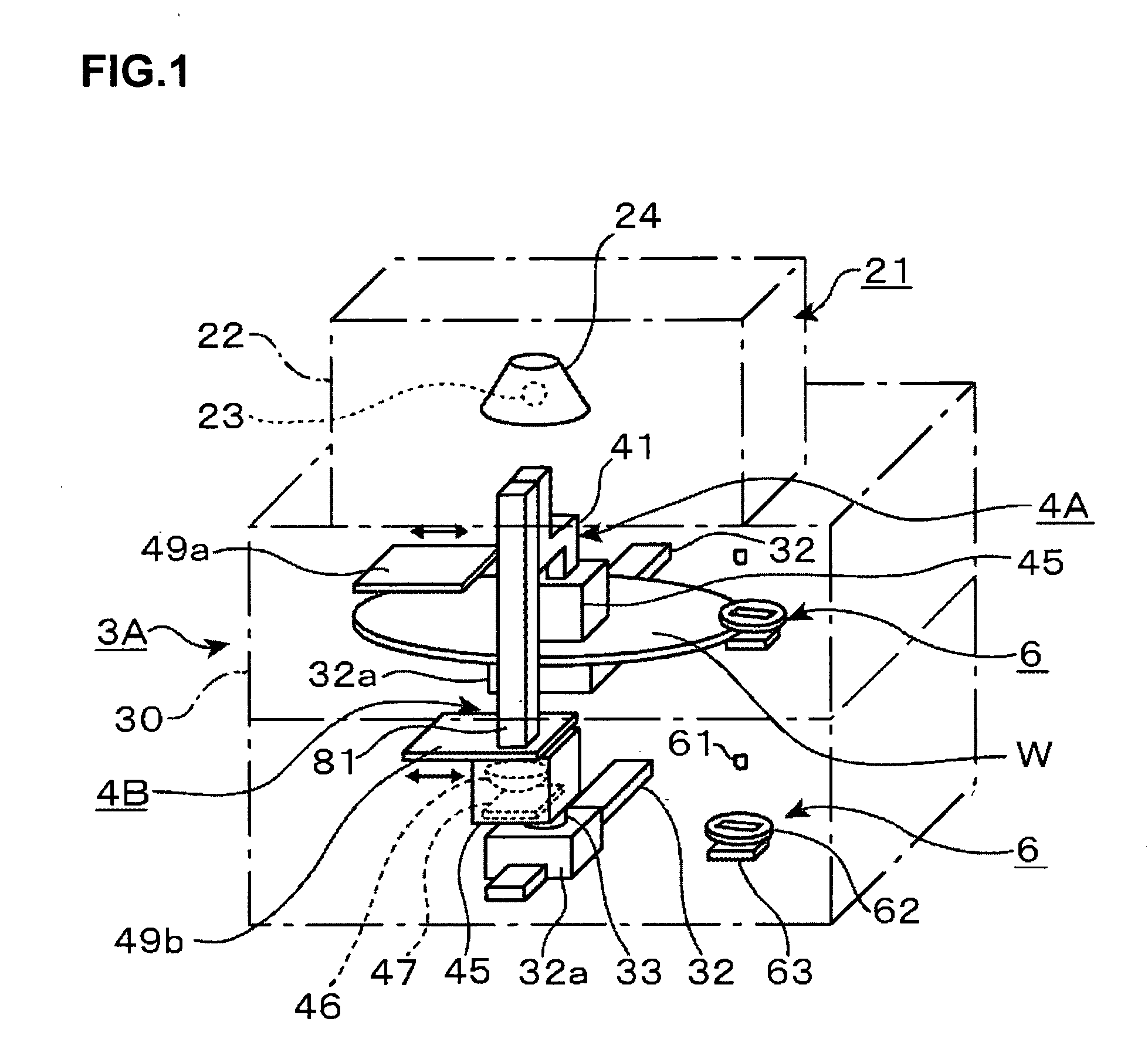
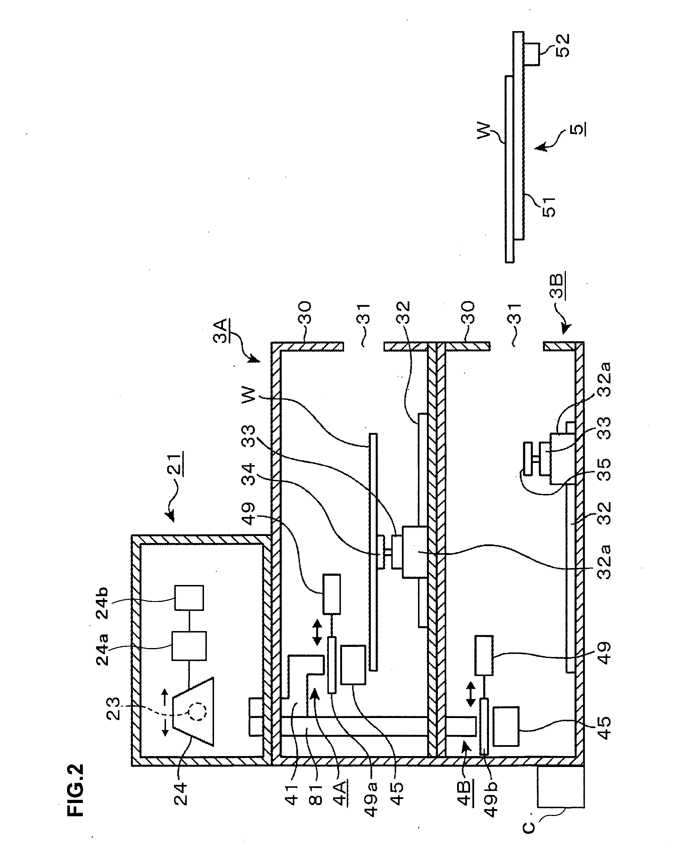
[0037] As an example of an embodiment of an edge exposure apparatus carrying out an edge exposure method relating to the present invention, an edge exposure apparatus 2 for exposing an edge portion of a semiconductor wafer W that is a substrate on which a resist film is formed by applying a resist solution being a coating solution of a photosensitive material to the surface will be described below with reference to FIG. 1 to FIG. 3. It should be noted that the wafer W used herein is provided with a notch N that is a cut-out portion indicating a position in a crystal orientation of the wafer W, for example, at the edge portion as shown in FIG. 3.

[0038] The edge exposure apparatus 2 comprises a light source unit 21, a first and a second exposure unit 3A and 3B, a first and a second optical path forming unit 4A and 4B, and an alignment unit 6. The light source unit 21 comprises, for example, a casing 22 in which a light source 23 radially emitting light employing, for example, a ultra...


PUM


Abstract

The present invention includes a first and a second optical path forming member arranged within a path of light beams from a light source; a first mounting table provided such that the edge portion of the substrate is located within an application region of the light beams from an outlet side of the first optical path forming member, and a second mounting table provided such that the edge portion of the substrate is located within an application region of the light beams from an outlet side of the second optical path forming member, each of the mounting tables being configured to be rotatable about a vertical axis while mounting the substrate thereon; and a light blocking means for blocking application of light from each of the first and second optical path forming members. A common light source can be used to perform edge exposure for the substrates on the first and second mounting tables, for example, at the same time, so that a high processing ability can be offered and an increase in size of the apparatus can be prevented.

Description

BACKGROUND OF THE INVENTION [0001] 1. Field of the Invention [0002] The present invention relates to an edge exposure apparatus for performing exposure for an edge portion of a substrate coated with a photosensitive material such as a resist or the like by applying light thereto, a coating and developing apparatus using the edge exposure apparatus, and an edge exposure method. [0003] 2. Description of the Related Art [0004] As an apparatus for forming a resist pattern on a substrate such as a semiconductor wafer (hereinafter, referred to as a wafer), for example, a coating and developing apparatus is employed which applies a photoresist (hereinafter, referred to as a resist) for the wafer and develops the wafer which has been exposed to light in an aligner. In this coating and developing apparatus, the application of the resist is performed in particular by supplying the resist onto the wafer being rotated so that the resist spreads over the front surface of the wafer by a centrifug...

Claims


Application Information

Patent Timeline
IPC IPC(8): G03B27/42
CPCG03F7/2022H01L21/67005G03F7/2028G03F7/2026H01L21/6715
Inventor IWASHITA, YASUHARUSHIMOMURA, ICHIRO
Owner TOKYO ELECTRON LTD
Why Eureka
Try Eureka