System and method for electrostatic discharge protection in an electronic circuit

a technology of electrostatic discharge protection and electronic circuit, which is applied in the direction of circuit electrostatic discharge protection, emergency protective arrangements for limiting excess voltage/current, and other directions, can solve the problems of large die area, inability to realize extensive die area, and inability to repair sensitive electronic circuits and any associated components, etc., to achieve less labor-intensive design and fabrication, less complicated circuitry of pcb or ic, and less pcb and/or ic.

Inactive Publication Date: 2006-11-09
AVAGO TECH WIRELESS IP SINGAPORE PTE
View PDF6 Cites 50 Cited by
  • Summary
  • Abstract
  • Description
  • Claims
  • Application Information

AI Technical Summary

Benefits of technology

[0010] Utilizing existing layers in a PCB or IC to realize an ESD protection scheme is advantageous for a number of reasons. For one, no additional layers need to be fabricated for the sole purpose of providing ESD protection. Furthermore, signal routing and signal paths become less complicated and intrusive as typically the ground plane and the battery plane are often prevalent throughout all areas of the PCB or IC. As a result, the circuitry of the PCB or IC becomes less complicated which results

Problems solved by technology

This electrostatic discharge (ESD) may create a transient voltage that, in turn, induces a transient current that may exceed maximum capacity thresholds for typical electronic circuits, thus, causing irreparable damage to sensitive electronic circuits and any associated components.
For example, an ESD event may cause a high-level transient voltage (typically as much as 16 kV) that will eventually cause damage to the protected component 110.
In each of theses cases, however, these ESD protection devices are fabricated as part of an integrated circuit (IC) and require extensive die area to be realized because of the nature of the components, i.e., diodes, resistors, etc.
When dealing with limited space in an IC, die area becomes an issue such that the ESD protection scheme may suffer for lack of available space on the IC.
Furthermore, these ESD devices are typically only realized on the top surface of the IC, thus requiring extensive signal routing for optimal ESD protection.
However, PCB space is again an issue as each additional SMT device requires at least one pin-out

Method used


Image

  • System and method for electrostatic discharge protection in an electronic circuit
  • System and method for electrostatic discharge protection in an electronic circuit
  • System and method for electrostatic discharge protection in an electronic circuit

Examples


Embodiment Construction

[0019] The following discussion is presented to enable a person skilled in the art to make and use the invention. The general principles described herein may be applied to embodiments and applications other than those detailed above without departing from the spirit and scope of the present invention. The present invention is not intended to be limited to the embodiments shown, but is to be accorded the widest scope consistent with the principles and features disclosed or suggested herein.

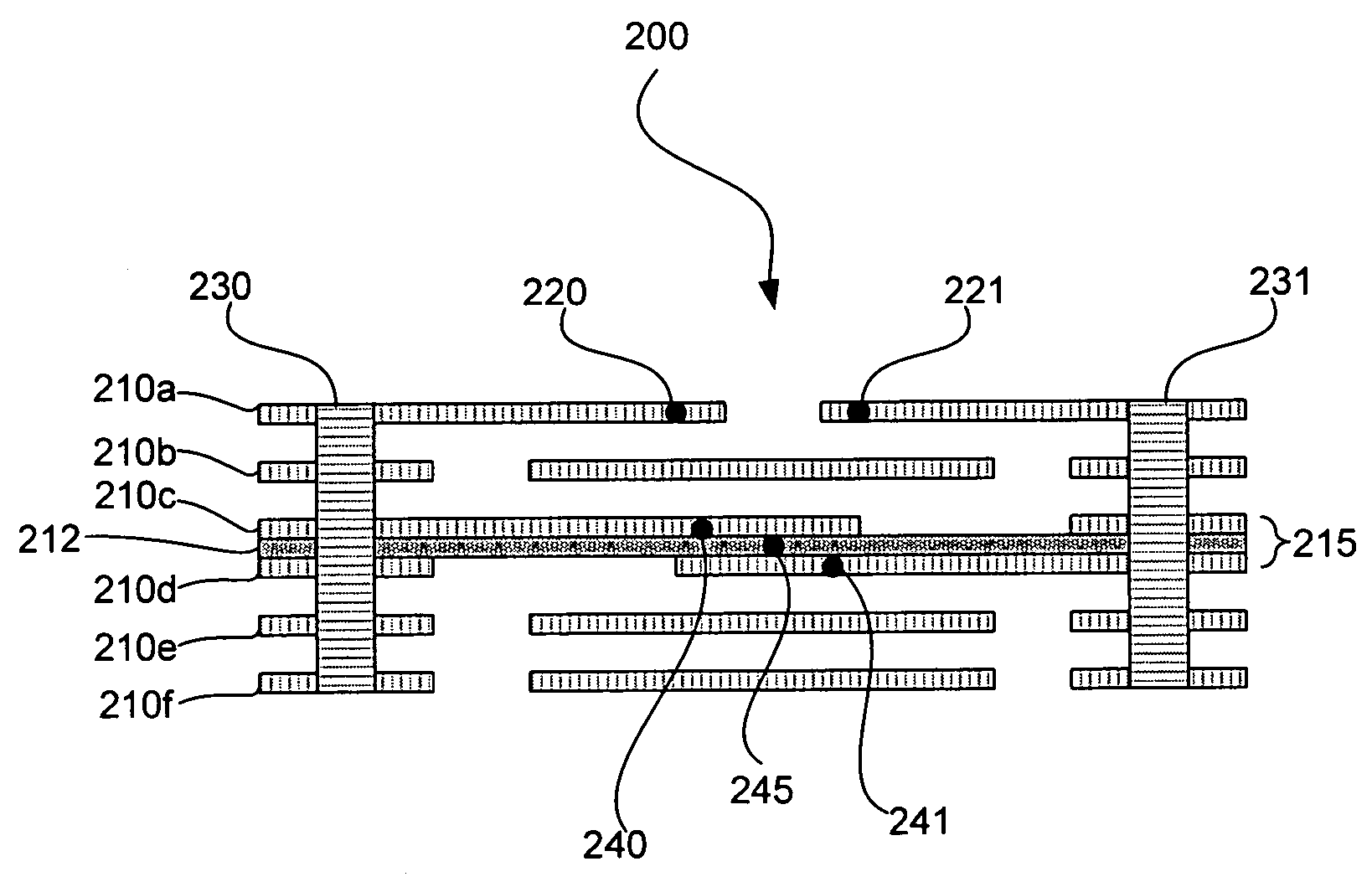
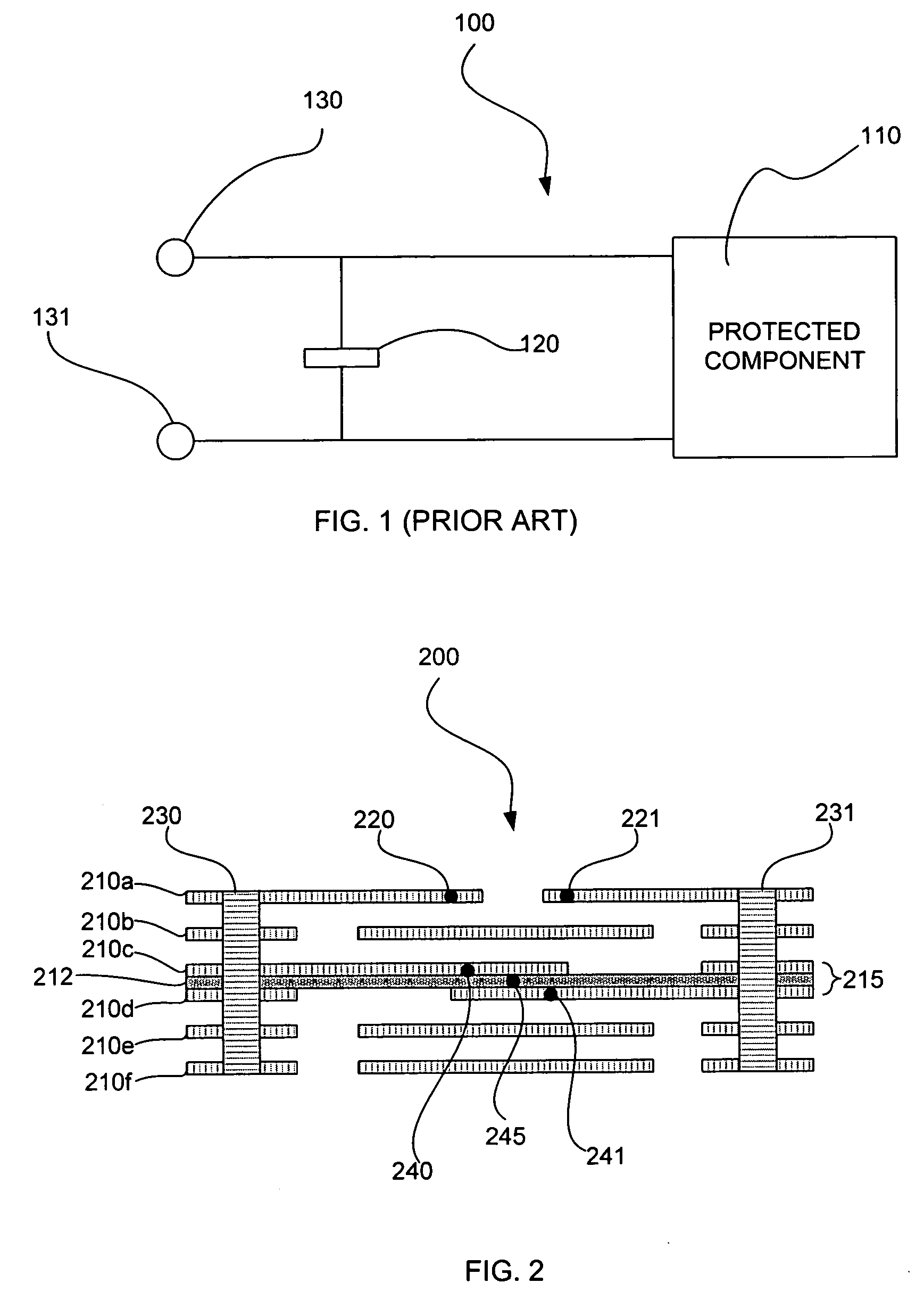
[0020]FIG. 2 is a cutaway view of a PCB 200 for diverting electrostatic discharge signals away from electronic components and the like according to an embodiment of the invention. A typical PCB 200 may include several layers 210 that may be fabricated to realize various interconnections and signal paths to, from, and through the PCB. In the embodiment of FIG. 2, the PCB 200 is shown with six distinct conductive plane layers 210a-210f. In this disclosure, these layers 210a-210f are simply named lay...


PUM


Abstract

A system and method for implementing an electronic circuit for protecting electronic components from ESD. A PCB or IC may include an electrostatic discharge protection layer having a first and second conductive layer separated by a semi-conductive dielectric layer. Further, the PCB/IC may include a protected node coupled to the first conductive layer and a current-shunt node electrically coupled to the second conductive layer, such that a signal at the protected node that is below a threshold magnitude propagates through the protected node in a normal operating path and a signal at the protected node that exceeds a threshold magnitude is diverted to the semi-conductive dielectric layer to the current-shunt node in a current-shunt path. In this manner, existing layers of a PCB/IC may be used for both ESD protection and other functions, such as ground planes or battery plane by isolating the specific sections of the layer for its intended use.

Description

BACKGROUND OF THE INVENTION [0001] Static electricity or static charge is the accumulated electric charge of an object that is typically an electric potential stored in the surface of the object that will discharge when presented with a conductive path to another object or ground. This electrostatic discharge (ESD) may create a transient voltage that, in turn, induces a transient current that may exceed maximum capacity thresholds for typical electronic circuits, thus, causing irreparable damage to sensitive electronic circuits and any associated components. Hence, this is the reason why printed circuit boards are always packaged and handled with anti-static plastic coverings. Additionally, typical electronic circuits include some form of ESD protection devices dealing with high-level transients. [0002]FIG. 1 is a conventional schematic diagram of an electronic circuit 100 having a typical ESD protection device that may be used to protect a component from excessive current levels th...

Claims


Application Information

Patent Timeline
IPC IPC(8): H02H9/00
CPCH01L23/62H05K1/0231H05K1/0259H05K1/0298H05K1/167H05K1/181H05K2201/09309H01L2924/0002H01L2924/00H01L23/60H05F3/00
Inventor PARKHURST, RAYRUEBUSCH, RONJIAA, CHISICKLER, JANET
Owner AVAGO TECH WIRELESS IP SINGAPORE PTE
Why Eureka
Try Eureka