Memory arrays using nanotube articles with reprogrammable resistance

a technology of reprogrammable resistance and memory array, which is applied in nanoinformatics, instruments, thermoelectric devices, etc., can solve the problems of low relative speed in comparison to dram or sram, low long-term reliability, and long write cycles (ms)

Active Publication Date: 2006-11-09
NANTERO
View PDF68 Cites 165 Cited by
  • Summary
  • Abstract
  • Description
  • Claims
  • Application Information

AI Technical Summary

Benefits of technology

[0038] Under another aspect, the first electrical stimulus includes applying one or more voltage pulses, wherein an amplitude of the pulses, a waveform of the pulses, and a number of the pulses together are sufficient to change the device to the first informational state. Under another aspect, the second electrical stimulus includes applying one or more voltage pulses, wherein an amplitude of the pulses, a waveform of the pulses, and a number of the pulses together are sufficient to change the device to the second informational state.

Problems solved by technology

ROM has a relatively low cost but cannot be rewritten.
EEPROM (or “Flash”) is inexpensive to produce and has low power consumption, but has long write cycles (ms) and low relative speed in comparison to DRAM or SRAM.
Flash also has a finite number of read / write cycles, which leads to low long-term reliability.
This complicates the system design, because separate circuitry must be included to “refresh” the memory contents both before the capacitors discharge, and after a read operation.
SRAM does not need to be refreshed, and is fast relative to DRAM, but has lower density and is more expensive relative to DRAM.
Both SRAM and DRAM are volatile, meaning that if power to the memory is interrupted, the memory cells will lose their stored information.
Consequently, existing commercially available technologies are generally either nonvolatile, but not randomly accessible and have a low density, high production cost, and a limited ability to allow multiple writes with high reliability of the circuit's function; or are volatile, and have complicated system design or have a low density.
A different proposed magnetic memory cell, based upon magnetic tunnel junctions, has also been examined but has not led to large-scale commercialized MRAM devices.
However FRAM memory cells tend to be large, and are difficult to manufacture as large-scale integrated components.
This technology, however, appears to operate at a slow speed, to be difficult to manufacture, has unknown reliability, and has not reached a state of commercialization.
This form of memory cell has the manufacturing limitation of requiring highly specialized wire junctions.
It also may not retain nonvolatility or long-term reliability owing to the inherent instability found in redox processes, and the risk of degradation of the chemical compound(s).

Method used


Image

  • Memory arrays using nanotube articles with reprogrammable resistance
  • Memory arrays using nanotube articles with reprogrammable resistance
  • Memory arrays using nanotube articles with reprogrammable resistance

Examples


Embodiment Construction

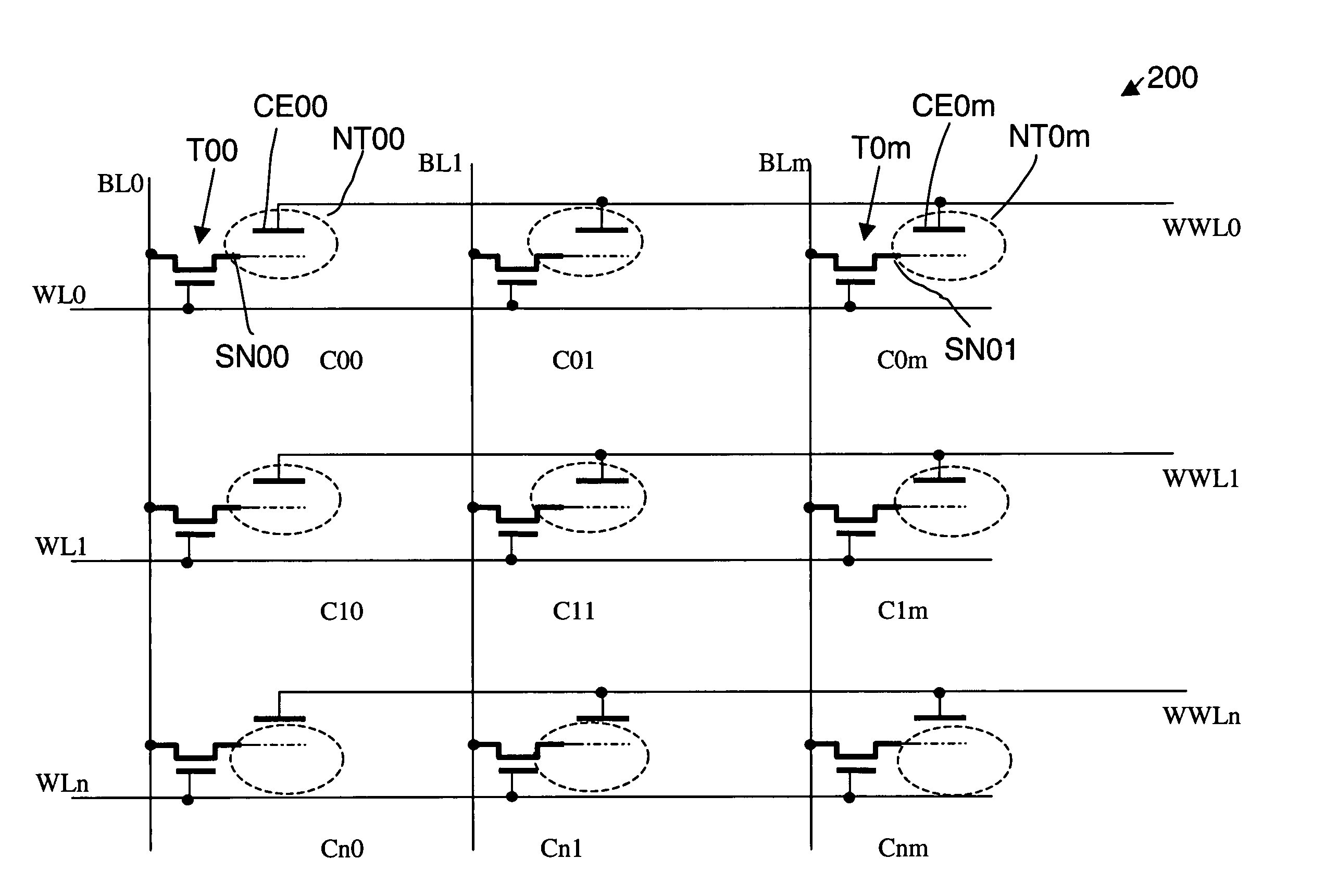
[0045] Preferred embodiments of the present invention provide scalable memory arrays that include nanotube articles with reprogrammable resistance. In general, the array includes a plurality of memory unit cells, each of which includes a cell selection transistor and a two-terminal nanotube switch, and is operably connected to a bit line, a first word line, and a second word line. The cell selection transistor is used to select the cell by applying an electrical stimulus to the transistor using the bit, first word, and / or the second word lines. The two-terminal nanotube switch is operably connected to the cell selection transistor, and is used to store the state of the memory unit cell. The two-terminal nanotube switch includes two conductive terminals and a nanotube element. The resistance between the two conductive terminals characterizes the state of the memory cell. A high resistance state can be used as a logic “0” state, and a low resistance state can be used as a logic “1” st...


PUM


Abstract

A memory array includes a plurality of memory cells, each of which receives a bit line, a first word line, and a second word line. Each memory cell includes a cell selection circuit, which allows the memory cell to be selected. Each memory cell also includes a two-terminal switching device, which includes first and second conductive terminals in electrical communication with a nanotube article. The memory array also includes a memory operation circuit, which is operably coupled to the bit line, the first word line, and the second word line of each cell. The circuit can select the cell by activating an appropriate line, and can apply appropriate electrical stimuli to an appropriate line to reprogrammably change the relative resistance of the nanotube article between the first and second terminals. The relative resistance corresponds to an informational state of the memory cell.

Description

CROSS-REFERENCE TO RELATED APPLICATIONS [0001] This application claims priority under 35 U.S.C. § 119(e) to the following applications, the contents of which are incorporated herein in their entirety by reference: [0002] U.S. Provisional Patent Application No. 60 / 679,029, filed on May 9, 2005, entitled Reversible Nanoswitch; [0003] U.S. Provisional Patent Application No. 60 / 692,891, filed on Jun. 22, 2005, entitled Reversible Nanoswitch; [0004] U.S. Provisional Patent Application No. 60 / 692,765, filed on Jun. 22, 2005, entitled Embedded CNT Switch Applications for Logic; and [0005] U.S. Provisional Patent Application No. 60 / 692,918, filed on Jun. 22, 2005, entitled NRAM Nonsuspended Reversible Nanoswitch Nanotube Array. [0006] This application is related to the following applications, the contents of which are incorporated herein in their entirety by reference: [0007] U.S. patent application No. (TBA), filed on an even date herewith, entitled Two-Terminal Nanotube Devices and System...

Claims


Application Information

Patent Timeline
Patent Type & Authority Applications(United States)
IPC IPC(8): G11C7/10
CPCB82Y10/00G11C13/0002G11C13/025G11C2213/79G11C2213/19G11C2213/35G11C2213/16
Inventor BERTIN, CLAUDE L.GUO, FRANKRUECKES, THOMASKONSEK, STEVEN L.MEINHOLD, MITCHELLSTRASBURG, MAXSIVARAJAN, RAMESHHUANG, X. M. HENRY
Owner NANTERO
Why Eureka
Try Eureka