Transparent member, optical device using transparent member and method of manufacturing optical device

a technology of transparent members and optical devices, applied in the direction of optical elements, instruments, lenses, etc., can solve the problems of difficult to pick up the lens, complicated management of inventory and processes, and damage to the lens, so as to improve production efficiency and quality

Inactive Publication Date: 2006-11-09
TOWA
View PDF11 Cites 60 Cited by
  • Summary
  • Abstract
  • Description
  • Claims
  • Application Information

AI Technical Summary

Benefits of technology

[0013] An object of the present invention is to provide a transparent member with improved production efficiency and quality, an optical device using the transparent member, and a method of manufacturing the optical device.
[0014] The transparent member of the present invention is, in an optical device having a substrate and a chip as an optical element mounted to the substrate, a transparent member used for the purpose of protecting the chip. The transparent member has a rectangular shape in plan view and is formed by dividing one integral molded body along phantom lines in a grid pattern. This structure allows a plurality of transparent members to be manufactured together, and therefore, increases the efficiency of manufacturing the transparent member. Furthermore, the transparent member has a rectangular shape in plan view so that it can be held by supporting its opposite sides. Therefore, errors occurring in handling of the transparent member and damages to it are prevented.
[0015] An optical device of one aspect of the present invention includes a substrate, a chip as an optical element mounted to the substrate, a protecting member provided on the substrate so as to surround the chip, and a transparent member attached to a top surface of the protecting member. Furthermore, the transparent member has a rectangular shape in plan view and is formed by dividing one integral molded body along phantom lines in a grid pattern. This structure can produce effects similar to those caused by the above-described transparent member.
[0017] An optical device of another aspect of the present invention includes a substrate, a chip as an optical element mounted to the substrate, and a sealing member with transparency provided at the substrate for the purpose of sealing the chip. In addition, the optical device is formed by dividing an intermediate body along phantom lines in a grid pattern. In this case, the intermediate body includes a whole substrate having a plurality of regions sectioned by the phantom lines in the grid pattern to correspond to the plurality of substrates, respectively, a plurality of chips mounted to the plurality of regions, respectively, and a whole sealing member having a plurality of sealing members corresponding to the plurality of regions, respectively, and integrally provided on the whole substrate. This structure also can improve the efficiency of manufacturing the optical device and facilitates handling of it.
[0020] Furthermore, the one molded body preferably includes a double-faced sheet having a base material, a temporary adhesive layer attached to one side of the base material and an actual adhesive layer attached to the other side of the base material and attached to the transparent member. In this case, the one molded body may be cut along the phantom lines with the temporary adhesive layer fixed to other members to form the plurality of transparent members, and after that, each of the plurality of transparent members may be removed from the base material. Then, the transparent member may be bonded to the top surface of the protecting member by the actual adhesive layer. This allows the manufacturing process to be simplified because it is not necessary to bond the transparent member to an opening using an adhesive.

Problems solved by technology

However, the conventional method set forth above poses the following problems.
This makes it difficult to pick up the lens by gripping or adsorption and the like and to handle the lens during transportation even if the lens has a small area of a flange portion.
In addition, if a jig for a handling operation contacts a portion through which light of the lens passes (transparent portion 10 in FIG. 25), the lens will be damaged.
Also, management of inventory and processes become complicated because it is necessary to store, pick up and transport individual lenses in all of the first to third manufacturing methods.
Furthermore, it is difficult to improve the efficiency of manufacturing LEDs because it is necessary to manufacture lenses and partially-completed products one by one and then attach one lens to one partially-completed product in all of the first to third manufacturing methods.

Method used


Image

  • Transparent member, optical device using transparent member and method of manufacturing optical device
  • Transparent member, optical device using transparent member and method of manufacturing optical device
  • Transparent member, optical device using transparent member and method of manufacturing optical device

Examples


first embodiment

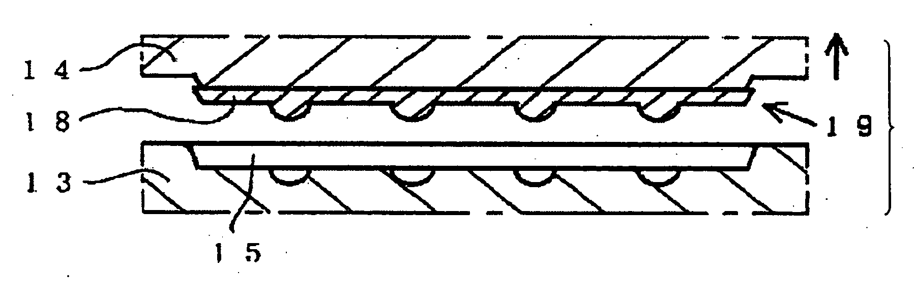
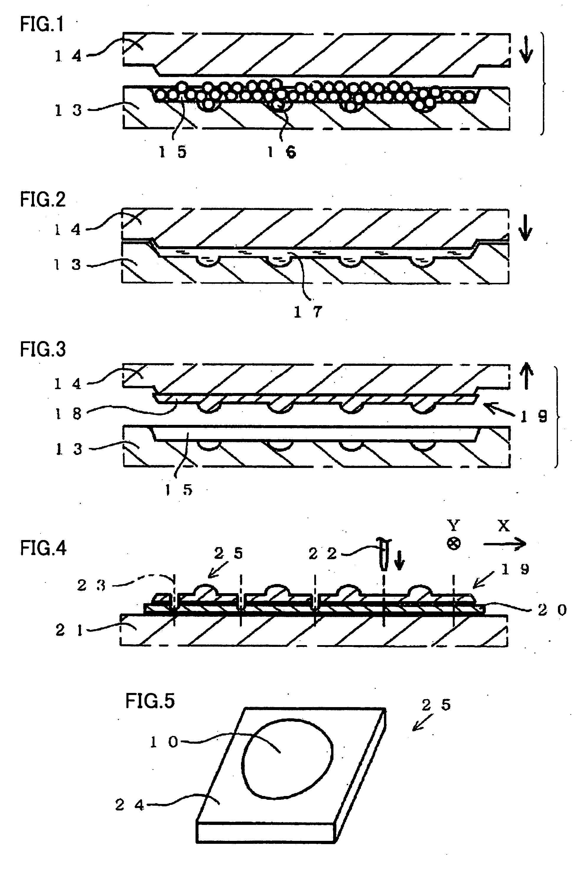
[0034] First, referring to FIGS. 1 to 5, a transparent member, an optical device and a method of manufacturing the optical device according to a first embodiment of the present invention will be described. In each drawing described below, the same components as those in FIGS. 21 to 25 are designated by the same reference characters. Furthermore, in the following description, an LED chip is used as an example of an optical element, and an LED package is used as an example of an optical device. However, the optical element of the present invention is not limited to the LED chip, and may be a light-receiving element converting received light to an electrical signal, for example, a chip such as a photodiode (PD) or a solid-state image sensor. Also, the optical element of the present invention may be a light-emitting element emitting light depending on received electrical signals, for example, a chip such as a laser diode (LD). In addition, the optical device of the present invention may...

second embodiment

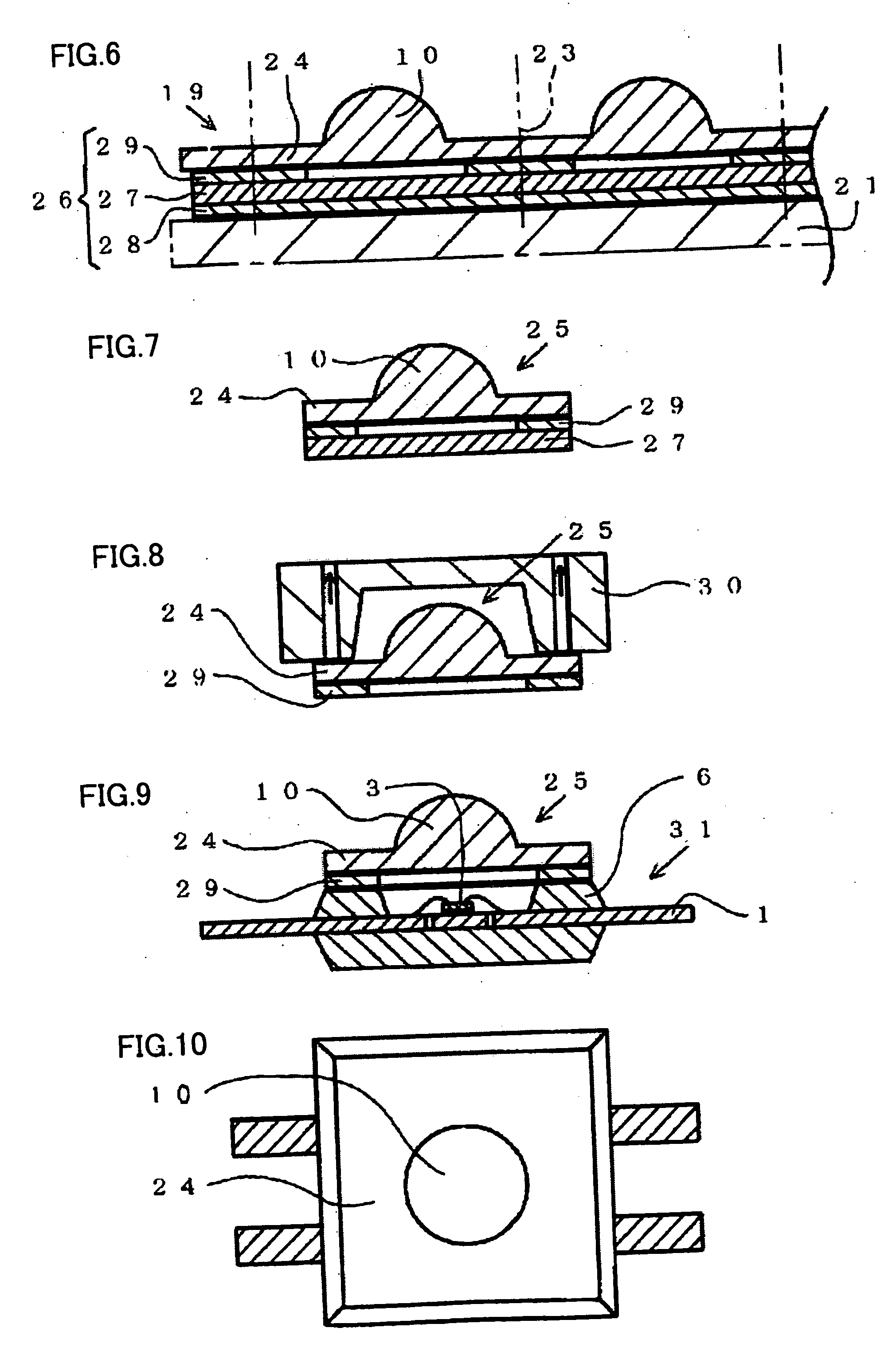
[0046] Referring to FIGS. 6 to 10, a transparent member, an optical device and a method of manufacturing the optical device according to a second embodiment of the present invention will be described. In the present embodiment, when a molded body is cut, it is temporarily fixed to a stage. In addition, each of a plurality of lens members formed by cutting the molded body is bonded to a corresponding partially-completed product. Also, by using a double-faced sheet, the molded body is temporarily fixed to the stage, and the lens member is bonded to the partially-completed product.

[0047] In the method of manufacturing the optical device of the present embodiment, as shown in FIG. 6, a double-faced sheet 26 is first affixed to the bottom side of a molded body 19. Double-faced sheet 26 has a three-layer structure which is constituted of a base material 27, a temporary adhesive layer 28 for temporary fixing which is formed on one side (the bottom side in FIG. 6) of base material 27 and h...

third embodiment

[0052] Then, referring to FIGS. 11 to 15, a transparent member, an optical device and a method of manufacturing the optical device according to a third embodiment of the present invention will be described. In the method of manufacturing the optical device of the present embodiment, as shown in FIG. 11, a whole substrate 33 is first prepared in which a plurality of regions 32 sectioned by phantom lines in a grid pattern and corresponding to optical devices, respectively, are formed. Note that whole substrate 33 includes a printed board and the like. Chips 3 are then die-bonded to regions 32 each having a rectangular shape in plan view, respectively, and electrodes (not shown) of chip 3 and whole substrate 33 are wire-bonded to each other by a wire 4.

[0053] Then, as shown in FIG. 12, a whole protecting member 34 surrounding a chip in each of the plurality of regions 32 is integrally formed by transfer molding. Note that, in place of this process, whole protecting member 34 may be in...


PUM


Abstract

In a method of manufacturing an optical device, a whole substrate is first prepared which has a plurality of regions corresponding to substrates constituting a plurality of optical devices, respectively. A plurality of chips are then mounted to the plurality of regions, respectively. A whole sealing member having a plurality of sealing members is integrally attached to the whole substrate to form an intermediate body. The intermediate body is divided into the above-described regions. Thus, the optical device having a substrate, a chip as an optical element mounted to the substrate and a sealing member with transparency provided at the substrate for the purpose of sealing the chip is manufactured. This manufacturing method improves the efficiency of manufacturing an optical device.

Description

[0001] This application is a Divisional of co-pending application No. 11 / 243,967, filed on Oct. 6, 2005, the entire contents of which are hereby incorporated by reference and for which priority is claimed under 35 U.S.C. §120.BACKGROUND OF THE INVENTION [0002] 1. Field of the Invention [0003] The present invention relates to a transparent member used in an optical device having a chip as an optical element, an optical device using the transparent member, and a method of manufacturing the optical device. [0004] 2. Description of the Background Art [0005] Referring to FIGS. 21 to 25, a first method of manufacturing a conventional optical device is described. Specifically, a method of manufacturing a package of a light-emitting diode (hereinafter referred to as an “LED”) is described as an example of a manufacturing method of the optical device. For the sake of simplicity, respective drawings in association with the description below are schematically depicted and not drawn to scale. [...

Claims


Application Information

Patent Timeline
Patent Type & Authority Applications(United States)
IPC IPC(8): H01L21/00H01L33/56H01L33/58H01L33/62
CPCG02B3/0031G02B3/0075H01L2224/73265H01L2224/32245H01L2924/12041H01L2924/01033H01L2924/01006H01L2924/01005H01L2924/01082H01L2224/97H01L2224/48247H01L2224/48091H01L33/58H01L24/97H01L2924/00014H01L2224/85H01L2924/00H01L2924/15787H01L2924/12043
Inventor ASHIDA, TAKESHI
Owner TOWA
Why Eureka
Try Eureka