Transmission electron microscope

a technology of electron microscope and transmission electron, which is applied in the direction of material analysis using wave/particle radiation, instruments, nuclear engineering, etc., can solve the problems of limiting the performance and usability affecting the accuracy of the electron microscope, and the influence of spherical aberration cannot be removed in principle, so as to reduce the time required, reduce the effect of false image effect, and easy and precise image interpretation

Inactive Publication Date: 2006-11-16
HITACHI LTD
View PDF0 Cites 5 Cited by
  • Summary
  • Abstract
  • Description
  • Claims
  • Application Information

AI Technical Summary

Benefits of technology

[0023] An object of the present invention is to provide a usable electron microscope which can reduce time required for observing condition setting in operation in the range from an unskilled to skilled person operating the electron microscope and obtain an electron microscope image in which image interpretation is easy and precise.
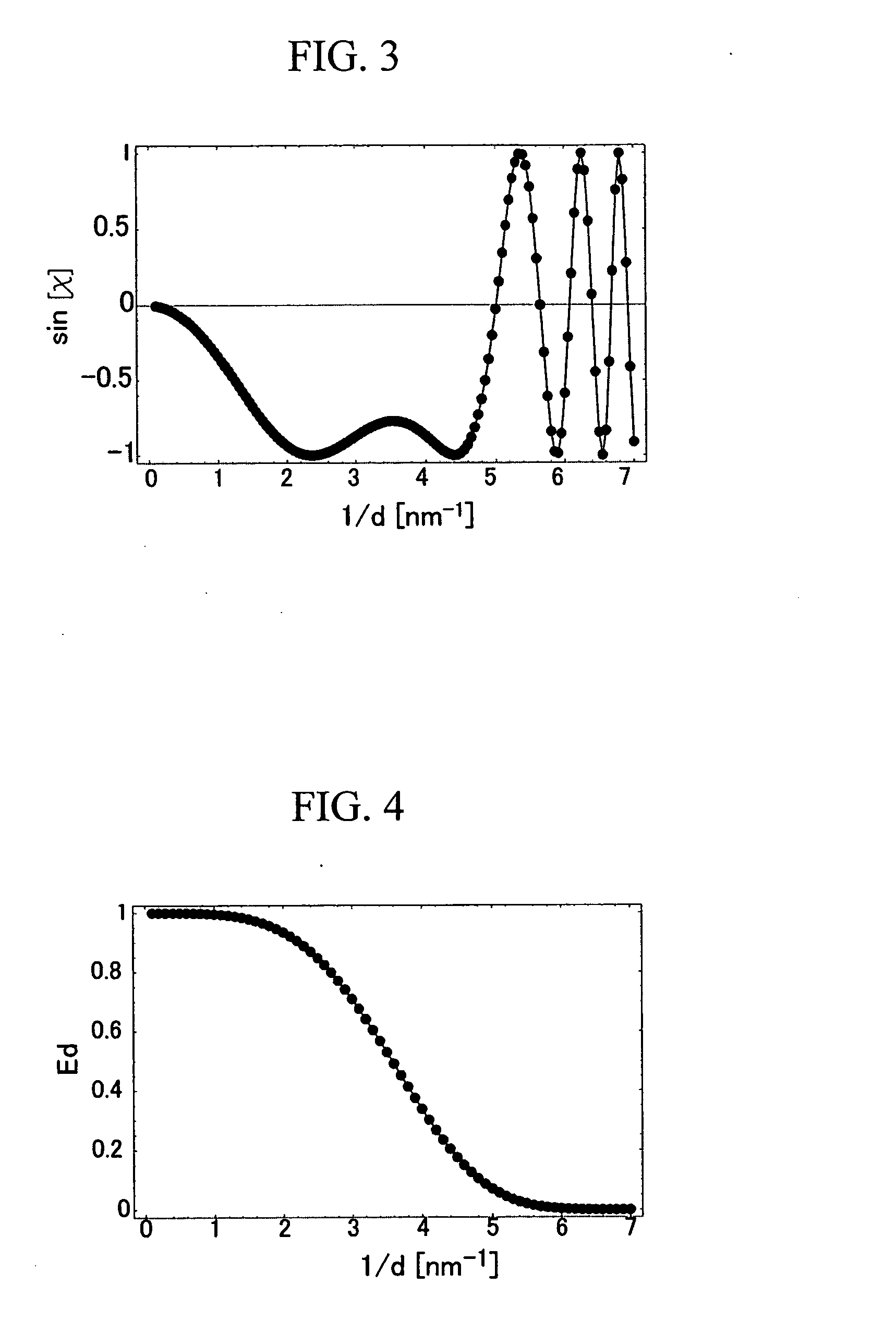
[0024] As an overall construction, an electron microscope has, in addition to an electron microscope main body, an inputting device for inputting a distance or spatial size d between any two points desired to be observed by an operator, and a calculating device for calculating a defocus amount Δfc of an objective lens in which contrast of an image corresponding to d is high and PCTF reducing a false image effect, and is provided with a function of showing the calculated PCTFs as plural candidates to the operator, and a means for automatically or manually selecting the PCTF whose phase inversion component has a relatively small intensity from these PCTFs. When one of the shown PCTFs is selected, a modulating signal (ΔV, ΔI, ΔId) for achieving reduction of the false image effect caused by the phase inversion component is calculated and a modulating signal based on the calculated result is generated by a modulator separated from the electron microscope body. A controller controls the entire electron microscope and also has a function of superimposing these generated modulating signals on an output of a high voltage power source, an objective lens power source, or a deflection coil power source in order to realize the modulating state. These systems are constructed and utilized to solve the above problems.
[0025] According to an embodiment of the present invention, when only the distance or spatial size d between any two points desired to be observed by the operator is known, a defocus amount of an objective lens achieving an electron microscope image based on this value at a high contrast can be automatically calculated and an observing condition for reducing or removing a false image effect caused by the spherical aberration of the objective lens can be semi-automatically set. Time spent on an image interpretation or a selecting operation of an objective aperture hole according to a specified spatial frequency desired to be noted, which has been the problem of the related art electron microscope observation experiment can be largely reduced. The related art method in which objective aperture holes have discrete hole diameters is limited to an object to be observed dimensioned closely to a discrete specified size corresponding to the hole diameter. The embodiment of the present invention needs not to be limited in this point and one electron microscope can cope with an object to be observed in a wide range.

Problems solved by technology

Nevertheless the image interpretations are difficult due to the false image effect, and often depend on the technical skill of the operator.
As far as using rotationally-symmetric magnetic field electron lenses, which are generally used in conventional electron microscopes, the influence of a spherical aberration can not be removed in principle.
This problem is an important factor to limit the performance and the usability of the electron microscope.
Even valid information can be blocked or unnecessary information cannot be prevented from being obtained.
In the former, the diameters and shapes of individual holes are required to have high accuracy and the inserted location of the objective aperture is spatially limited.

Method used


Image

  • Transmission electron microscope
  • Transmission electron microscope
  • Transmission electron microscope

Examples


Embodiment Construction

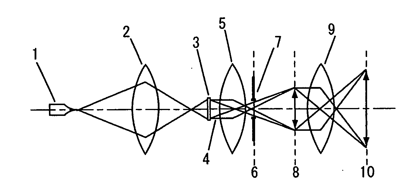
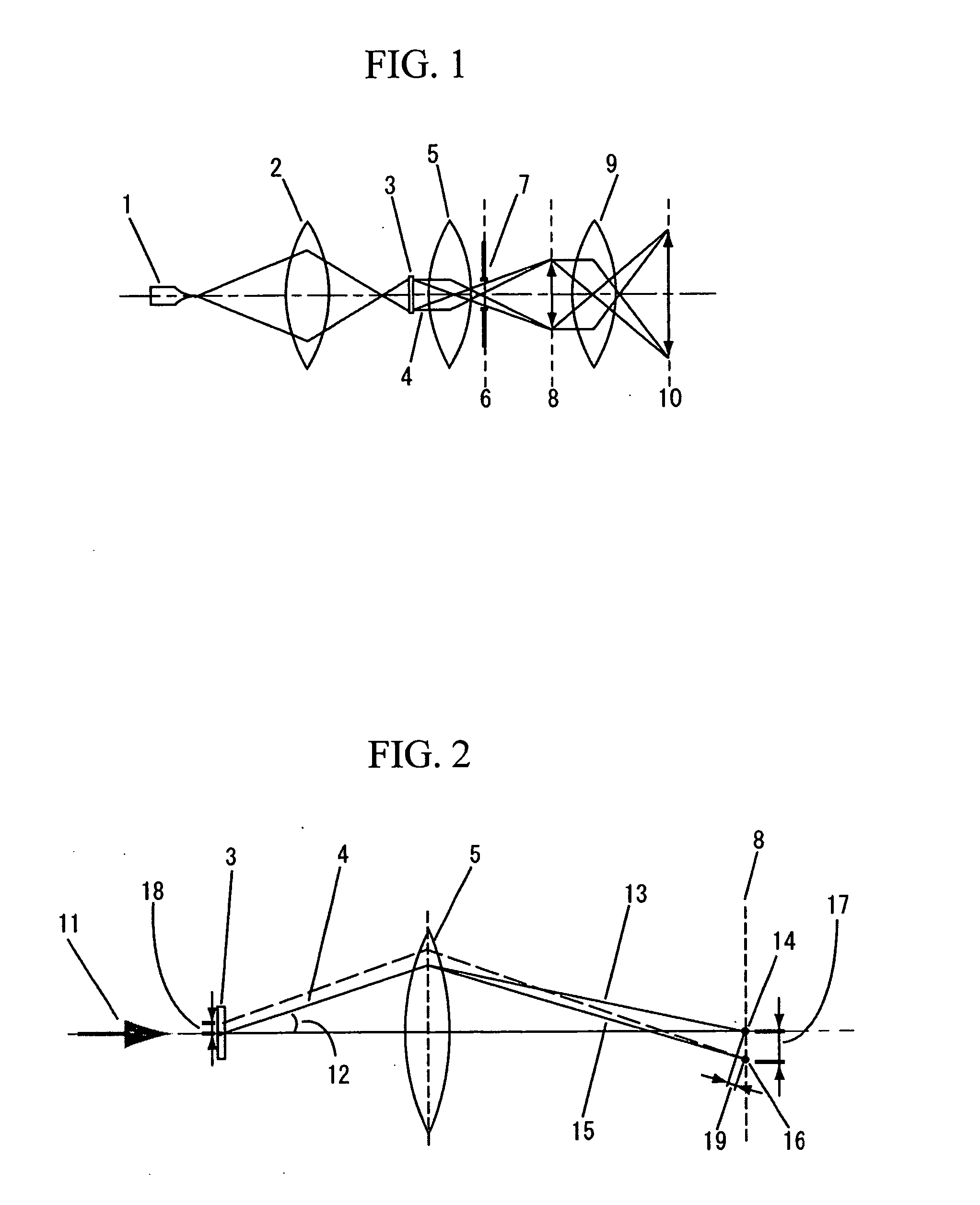
[0041]FIG. 10 shows the overview of a device embodying the present invention. An electron gun 20 has an electron source 1 constructed of a needle-like tungsten single crystal whose edge is sharpened, an extractor electrode 21 placed in a position opposite thereto, and an acceleration tube 22 for accelerating an extracted electron. A high voltage can be applied to the extractor electrode 21 by an extractor power source 23 provided externally and electrons can be extracted by applying a voltage of about −3.0 to −2.5 kV between the extractor electrode 21 and the electron source 1.

[0042] An accelerating voltage for accelerating an extracted electron is supplied to the acceleration tube 22 by an accelerating voltage source 24. An electron beam emerged from the electron gun 20 is set to a desired illuminating condition by an illumination lens 2 supplied with an exciting current from an illumination lens power source 25. An output of a deflection coil power source 27 supplying an electric...


PUM


Abstract

A transmission electron microscope has a means for inputting a spatial size or distance d desired to be observed by the operator, calculates high contrast of an image based on this value and an observing condition which can reduce the influence of a false image superimposed, and desirably modulates an accelerating voltage of the electron microscope based thereon.

Description

CLAIM OF PRIORITY [0001] The present application claims priority from Japanese application JP 2005-136803 filed on May 10, 2005, the content of which is hereby incorporated by reference into this application. BACKGROUND OF THE INVENTION [0002] 1. Field of the Invention [0003] The present invention relates to a transmission electron microscope. In particular, the present invention relates to a transmission electron microscope and an image observing method using the same. More specifically, the present invention relates to an observing method which improves the quality of an electron microscope image obtained by a transmission electron microscope having a highly bright and coherent electron source. [0004] 2. Description of the Related Art [0005] A transmission electron microscope which is a device illuminating a sample by an electron beam and forming a magnified image by electron lenses with a transmitted electron beam, enables us to directly observe fine structures in the sample. The...

Claims


Application Information

Patent Timeline
Patent Type & Authority Applications(United States)
IPC IPC(8): G21K7/00
CPCH01J37/21H01J37/26H01J2237/2487H01J37/265H01J37/263
Inventor KASAI, HIROTOYOSHIDA, TAKAHO
Owner HITACHI LTD
Why Eureka
Try Eureka