Compact via transmission line for printed circuit board and its designing method

a technology of printed circuit board and transmission line, which is applied in the direction of printed element electric connection formation, high frequency circuit adaptation, waveguide, etc., can solve the problems of inevitably occurring difficult problems, and achieve the effect of expanding the frequency range of the via transmission lin

Active Publication Date: 2006-11-16
RENESAS ELECTRONICS CORP +1
View PDF3 Cites 72 Cited by
  • Summary
  • Abstract
  • Description
  • Claims
  • Application Information

AI Technical Summary

Benefits of technology

[0009] It is therefore a primary object of the present invention to achieve a miniaturized via transmission line with preferred characteristic impedance suitable for high-density mounting, as well as to extend the frequency range of a via transmission line in a printed circuit board including a multilayer printed circuit board.

Problems solved by technology

However, while it is essential to accurately carry out impedance matching with respect to a via transmission line comprising one signal via hole and the barrier of the ground via holes in a case where the composite via transmission line is miniaturized, the fact is that a difficult problem that inevitably arises occurs.

Method used


Image

  • Compact via transmission line for printed circuit board and its designing method
  • Compact via transmission line for printed circuit board and its designing method
  • Compact via transmission line for printed circuit board and its designing method

Examples


Embodiment Construction

[0065] Hereinafter, an overview of the embodiment of the present invention will be described.

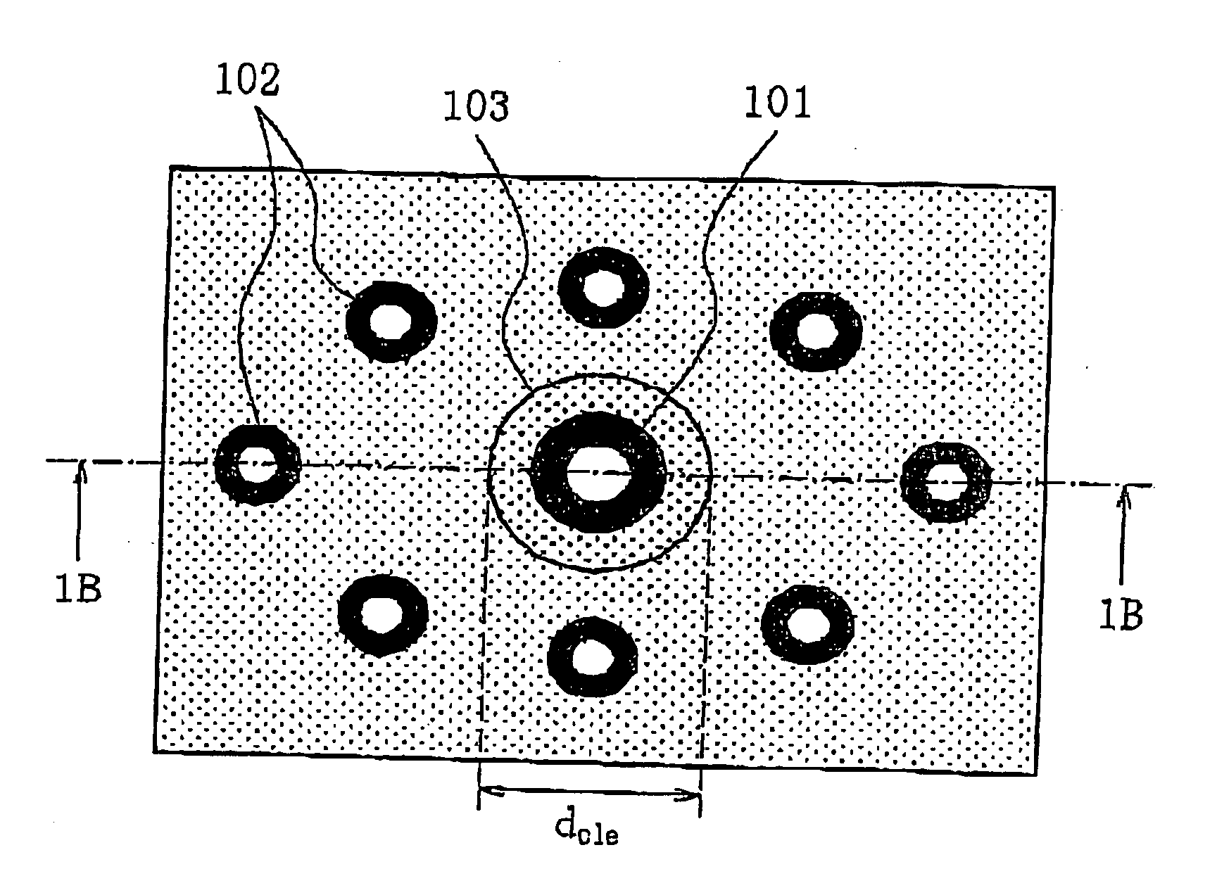
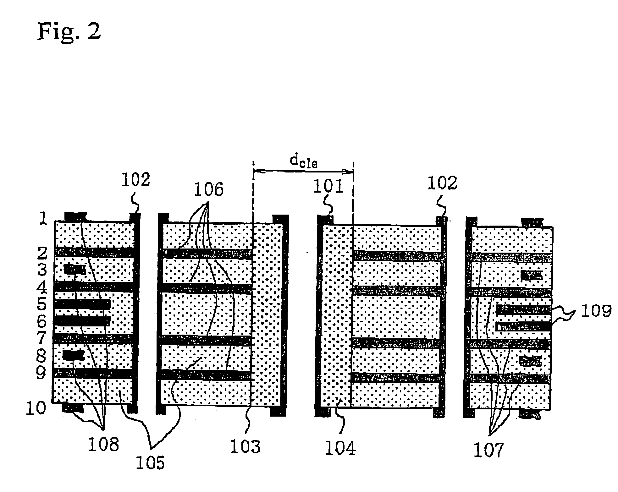
[0066] The compact via transmission line according to the present invention has a central conductor which forms an inner conductor layer boundary of the compact via transmission line, a plurality of ground via holes arranged around the signal via and a set of ground plates from conductor layers of a printed circuit board to form all outer conductor boundary of the compact via transmission line, and a constitutive parameter adjustment via hole for electrically isolating the inner conductor boundary from the outer conductor boundary which have differential potentials. This constitutive parameter adjustment via hole may be filled with a composite material made of a uniform substance or a plurality of different substances. A particular example includes a method of forming air vents between a signal via and ground via holes of a via transmission line to adjust a constitutive parameter of a print...


PUM


Abstract

A compact via transmission line for a printed circuit board having preferred characteristic impedance and capable of miniaturizing the printed circuit board including a multilayer printed circuit board, and extending the frequency range of a via transmission line mounted on the printed circuit board, and a design method of the same. The transmission line has a central conductor forming an inner conductor layer boundary make up a signal via hole, a plurality of via holes arranged around the central conductor form an outer conductor layer boundary, and a plurality of conductor plates formed of a printed circuit board conductor layer, is further provided with a constitutive parameter adjustment clearance hole between the inner and outer conductor layer boundaries of the compact via transmission line, and electrically isolates to prevent cross-talk of a signal propagating through a signal via hole with other signals in a high-frequency signal band.

Description

TECHNICAL FIELD [0001] The present invention relates to a compact via transmission line for a printed circuit board and a design method of the same, and in particular to a miniaturized compact via transmission line for a printed circuit board in which constitutive parameters of medium filling the clearance hole of the via transmission line such as relative permittivity and relative permeability are different from the constitutive parameter of an insulating layer comprising the printed circuit board, and a design method of the same. BACKGROUND ART [0002] For the purpose of more adequately describing a technological level for the present invention at present, all descriptions of the patents, patent applications, patent gazettes, scientific papers, and the like which are cited or specified in the present application will be incorporated herein by reference. [0003] Interconnected circuits are very important for improvement in speeding up and packing density of a digital device and a com...

Claims


Application Information

Patent Timeline
Patent Type & Authority Applications(United States)
IPC IPC(8): H01P5/02H01P3/06H05K1/02H05K3/42
CPCH01P3/06H05K1/0222H05K1/024H05K1/0251H05K3/429H05K2201/09809H05K2201/09063H05K2201/09536H05K2201/09618H05K2201/09718H05K2201/0187
Inventor KUSHTA, TARASNARITA, KAORUSAEKI, TAKANORIKANEKO, TOMOYUKITOHYA, HIROKAZU
Owner RENESAS ELECTRONICS CORP
Why Eureka
Try Eureka