This helps you quickly interpret patents by identifying the three key elements:
Problems solved by technology
Method used
Benefits of technology
Benefits of technology
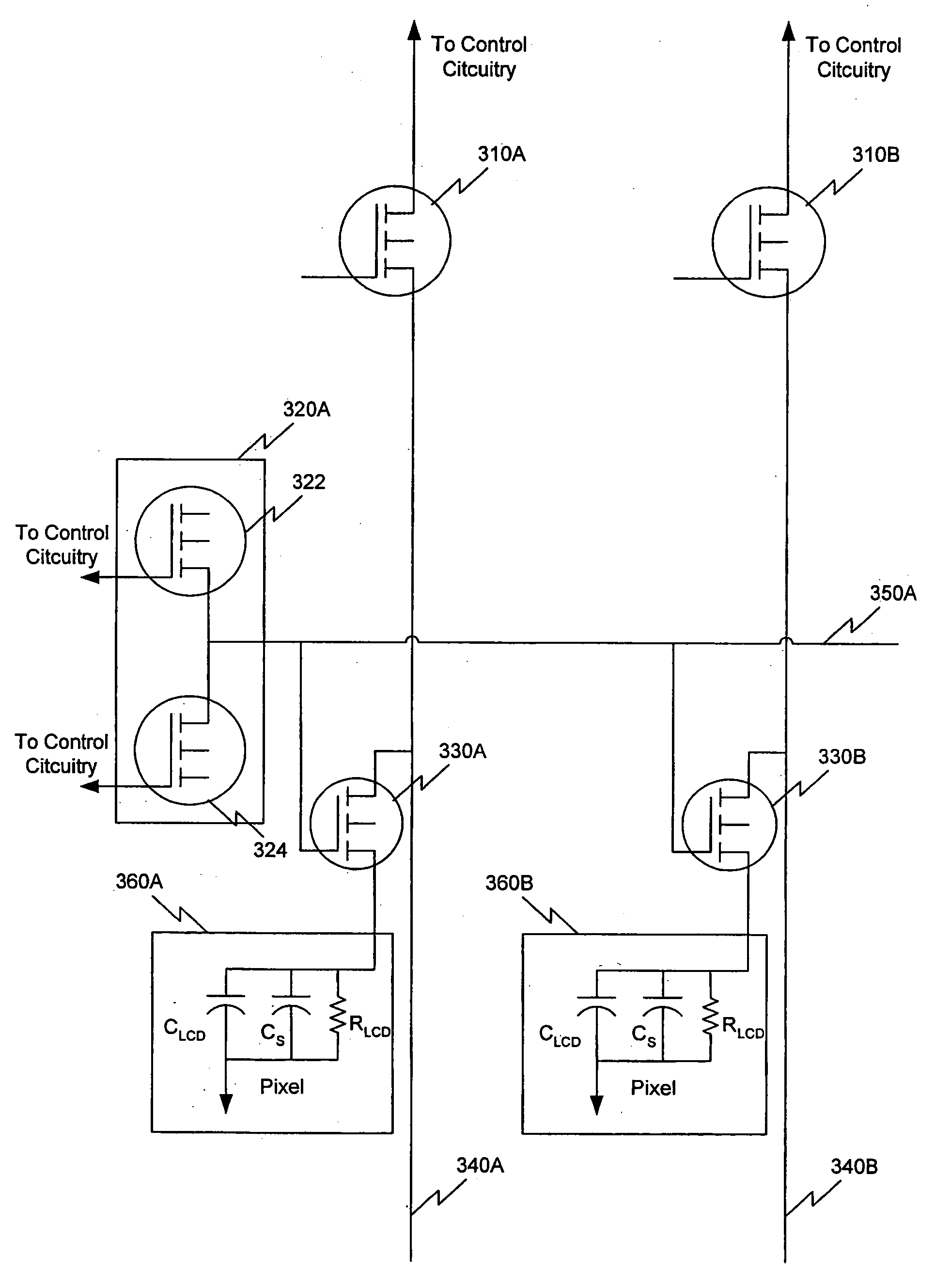
[0014] There are numerous benefits associated with the use of nanowire transistors within a display. First, nanowire transistors can be positioned on a multitude of substrates including glasses and plastics. As a result, displays can be developed on flexible substrates that open up a plethora of applications using flexible and / or rollable displays. Second, nanowire transistors have superior performance when compared to a-Si and poly-Si TFTs, thereby allowing the edge electronics associated with the row and column transistors to be integrated between the row and column traces. This allows displays, in particular LCDs, to be produced with an increased ratio of screen size to frame size for holding the screen and reduces the complexity of external control circuitry. Furthermore, because nanowire transistors are small they reduce obscuration associated with conventional a-Si and poly Si TFTs that is typically quite poor, since the larger a-Si and poly Si TFTs tend to block a significant portion of the light being reflected or transmitted through a display, such as an LCD. For emissive displays like OLEDs, smaller transistors allow a larger portion of the backplane area to be occupied by the OLEDs constructed directly on the backplane, rather than the more difficult process of building the OLEDs on top of the pixel transistor
Problems solved by technology
Furthermore, because nanowire transistors are small they reduce obscuration associated with conventional a-Si and poly Si TFTs that is typically quite poor, since the larger a-Si and poly Si TFTs tend to block a significant portion of the light being reflected or transmitted through a display, such as an LCD.
Method used
Image
Click on the blue label to locate the original text in one second.
Reading with bidirectional positioning of images and text.
Examples
Embodiment Construction
[0024] It should be appreciated that the particular implementations described herein are examples of the invention and are not intended to otherwise limit the scope of the present invention in any way. Indeed, for the sake of brevity, conventional electronics, manufacturing, semiconductor devices, and nanotube, nanorod, nanowire and nanoribbon technologies and other functional aspects of the systems (and components of the individual operating components of the systems) may not be described in detail herein. Moreover, while the number of nanowires and spacing of those nanowires are provided for the specific implementations discussed, the implementations are not intended to be limiting and a wide range of the number of nanowires and spacing can also be used. Furthermore, dimensions and compositions of the nanowires can be varied. The implementations described are not intended to be limiting and a wide range of dimensions and compositions can be used.
[0025] As used herein, the term “n...
PUM
Property
Measurement
Unit
length:width
aaaaa
aaaaa
length:width
aaaaa
aaaaa
aspect ratio
aaaaa
aaaaa
Abstract
The present invention is directed to a display using nanowire transistors. In particular, a liquid crystal display using nanowire pixel transistors, nanowire row transistors, nanowire column transistors and nanowire edge electronics is described. A nanowire pixel transistor is used to control the voltage applied across a pixel containing liquid crystals. A pair of nanowire row transistors is used to turn nanowire pixel transistors that are located along a row trace connected to the pair of nanowire row transistors on and off. Nanowire column transistors are used to apply a voltage across nanowire pixel transistors that are located along a column trace connected to a nanowire column transistor. Displays including organic light emitting diodes (OLED) displays, nanotube field effect displays, plasma displays, micromirror displays, micoelectromechanical (MEMs) displays, electrochromic displays and electrophoretic displays using nanowire transistors are also provided.
Description
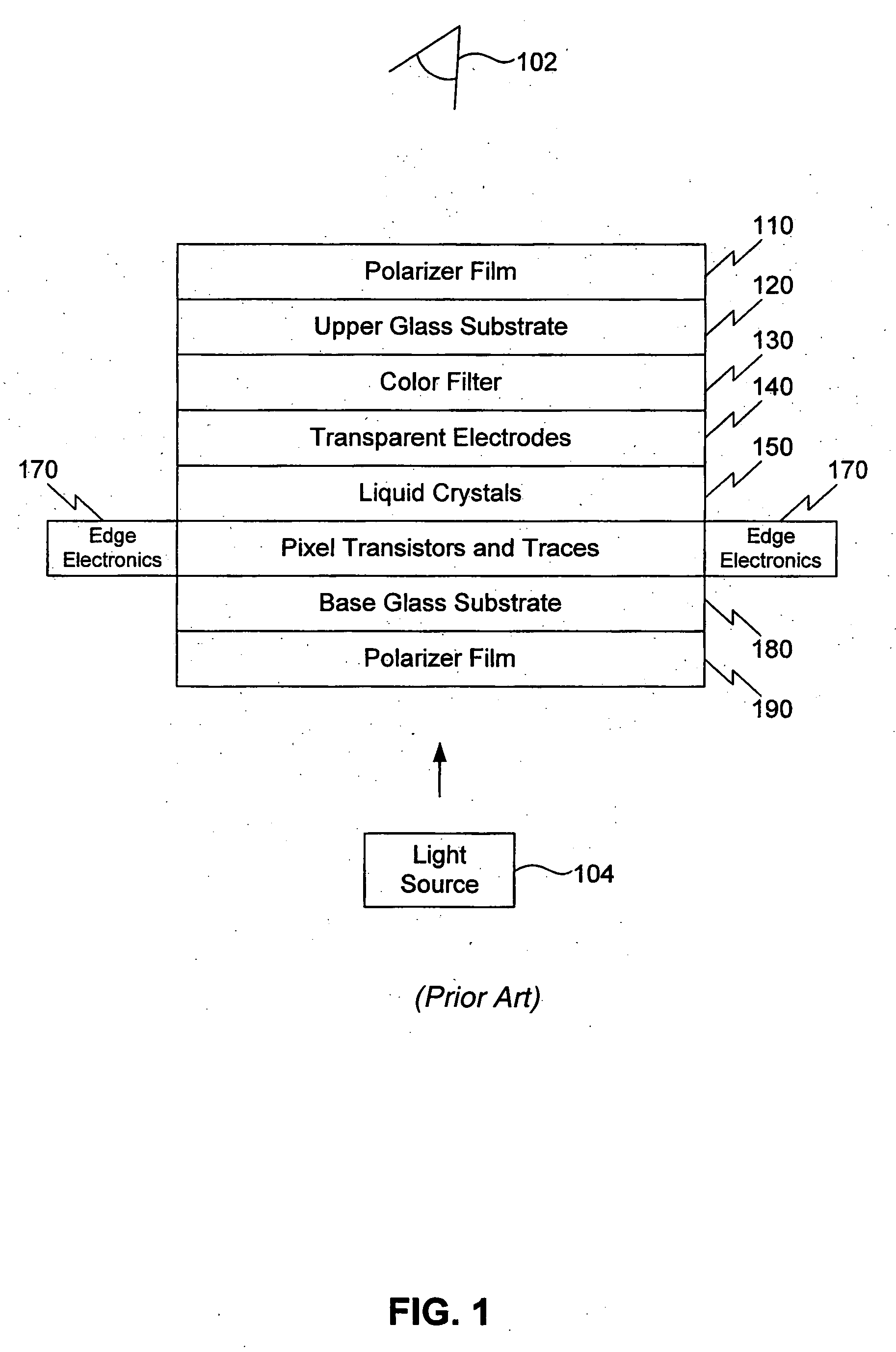
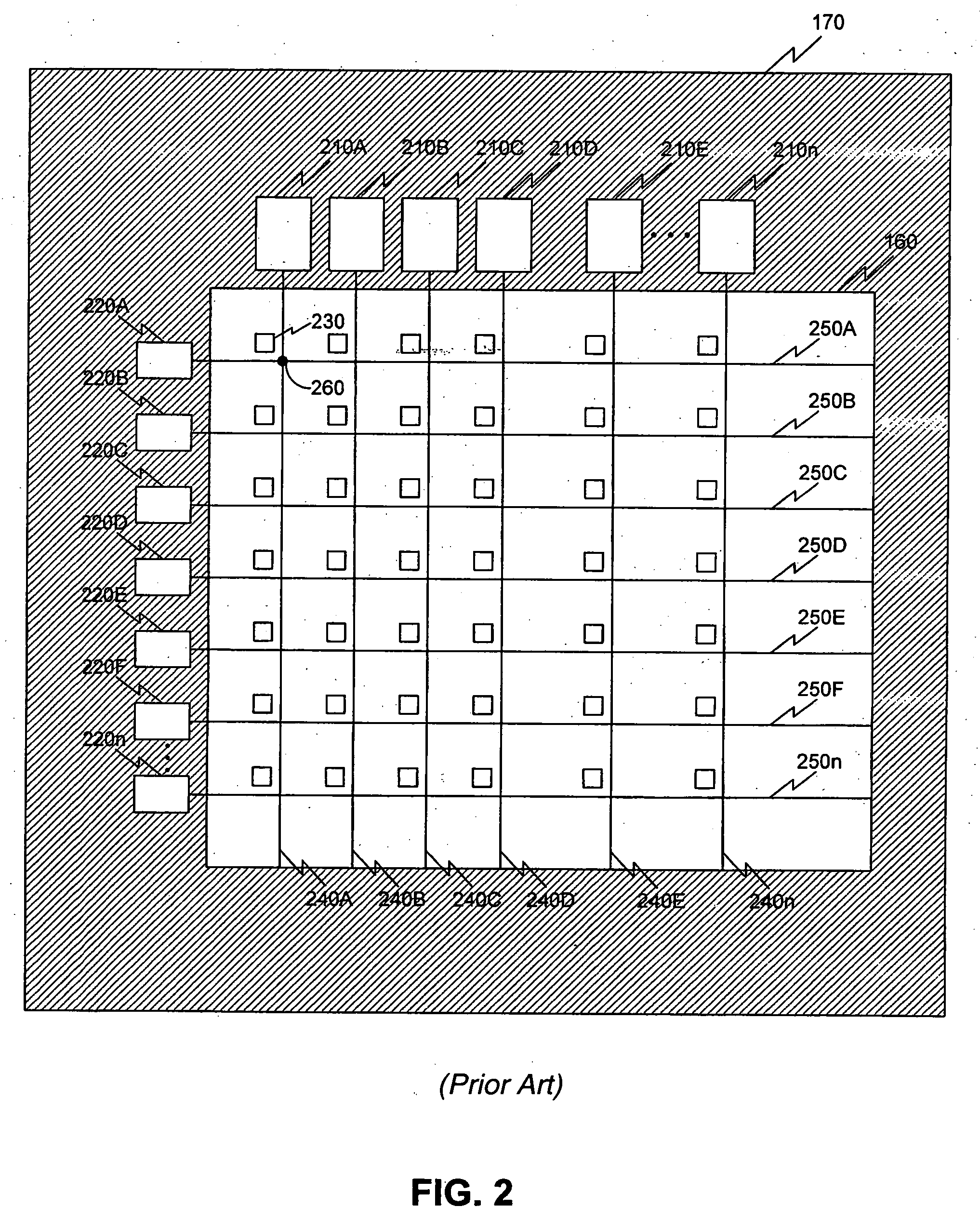
CROSS-REFERENCE TO RELATED APPLICATIONS [0001] This application is a continuation of U.S. patent application Ser. No. 10 / 673,669, filed Sep. 30, 2003, which is hereby incorporated herein in its entirety; which claims the benefit of U.S. Provisional Application Nos. 60 / 488,801, filed Jul. 22, 2003, which is hereby incorporated herein in its entirety; 60 / 414,323, filed Sep. 30, 2002, which is hereby incorporated herein in its entirety; 60 / 414,359, filed Sep. 30, 2002, which is hereby incorporated herein in its entirety; and 60 / 468,276, filed May 7, 2003, which is hereby incorporated herein in its entirety.BACKGROUND OF THE INVENTION FIELD OF THE INVENTION [0002] The present invention relates to displays, and more particularly, integrated displays using nanowire transistors. [0003] A wide variety of display technologies exist. These display technologies include liquid crystal displays, organic light emitting diodes (OLED) displays, nanotube field effect displays, plasma displays, micro...
Claims
Application Information
Patent Timeline
Application Date:The date an application was filed.
Publication Date:The date a patent or application was officially published.
First Publication Date:The earliest publication date of a patent with the same application number.
Issue Date:Publication date of the patent grant document.
PCT Entry Date:The Entry date of PCT National Phase.
Estimated Expiry Date:The statutory expiry date of a patent right according to the Patent Law, and it is the longest term of protection that the patent right can achieve without the termination of the patent right due to other reasons(Term extension factor has been taken into account ).
Invalid Date:Actual expiry date is based on effective date or publication date of legal transaction data of invalid patent.
Patent Type & AuthorityApplications(United States)

