Photovoltaic element and method of producing photovoltaic element

a photovoltaic element and photovoltaic element technology, applied in the field of photovoltaic elements, can solve the problems of increasing resistance loss with the increasing length of the current-collecting electrode, the inability to fill the light-receiving surface of the photovoltaic element module, and the inability to effectively utilize the light-receiving surface area, etc., to achieve the effect of facilitating series connection, facilitating reliability of the photovoltaic element, and enhancing the degree of freedom

Inactive Publication Date: 2006-11-23
CANON KK
View PDF8 Cites 61 Cited by
  • Summary
  • Abstract
  • Description
  • Claims
  • Application Information

AI Technical Summary

Benefits of technology

[0036] According to the present invention, by connecting the rear surface side bus-bar electrode to the metal substrate at a portion corresponding to the island-shaped transparent-electrode-layer-removed-portion, only a region in which the semiconductor element may be deteriorated due to connection working of the rear surface side bus-bar electrode can be electrically separated from the transparent electrode layer in the other portion of the power-generating region (the region surrounded by the etching line in which the peripheral portion of the transparent electrode layer is continuously removed), so that the reliability of the photovoltaic element can be ensured. As a result, when in order to facilitate series connection in a widthwise direction of the photovoltaic elements, the rear surface side bus-bar electrode is disposed so as to be offset in a lateral direction with respect to the bus-bar electrode provided on the surface of the photovoltaic element, there can be obtained a technical effect that the degree of freedom for the shape of a photovoltaic element module is enhanced while the reliability of the photovoltaic element is ensured.

Problems solved by technology

There is nuclear power generation as one of such energy sources, but it has many problems to be solved such as radioactive waste, and there is an increasing demand for a clean energy source having a higher degree of safety.
As a result, the light-receiving surface of the photovoltaic element module cannot always be filled with photovoltaic elements without leaving a gap to be utilized effectively.
On the other hand, the standard dimension of a photovoltaic element is increasingly enlarged in order to reduce the production cost, which increasingly enlarges odd gaps incapable of disposing the photovoltaic element therein, thus making it difficult to effectively utilize the light-receiving surface area.
This is because a material constituting a current-collecting electrode of a photovoltaic element does have some finite resistance value, and as a result, the resistance loss increases with the increasing length of the current-collecting electrode.
However, it has been found that because such electrode configuration makes a bus-bar electrode provided on the rear surface be positioned in the rear surface of the power-generating region of a photovoltaic element, if the rear surface side bus-bar electrode is connected by some working in such a state, there is posed a problem that the element in the power-generating region may be deteriorated or broken.

Method used


Image

  • Photovoltaic element and method of producing photovoltaic element
  • Photovoltaic element and method of producing photovoltaic element
  • Photovoltaic element and method of producing photovoltaic element

Examples


example 1

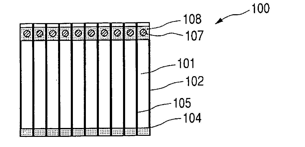
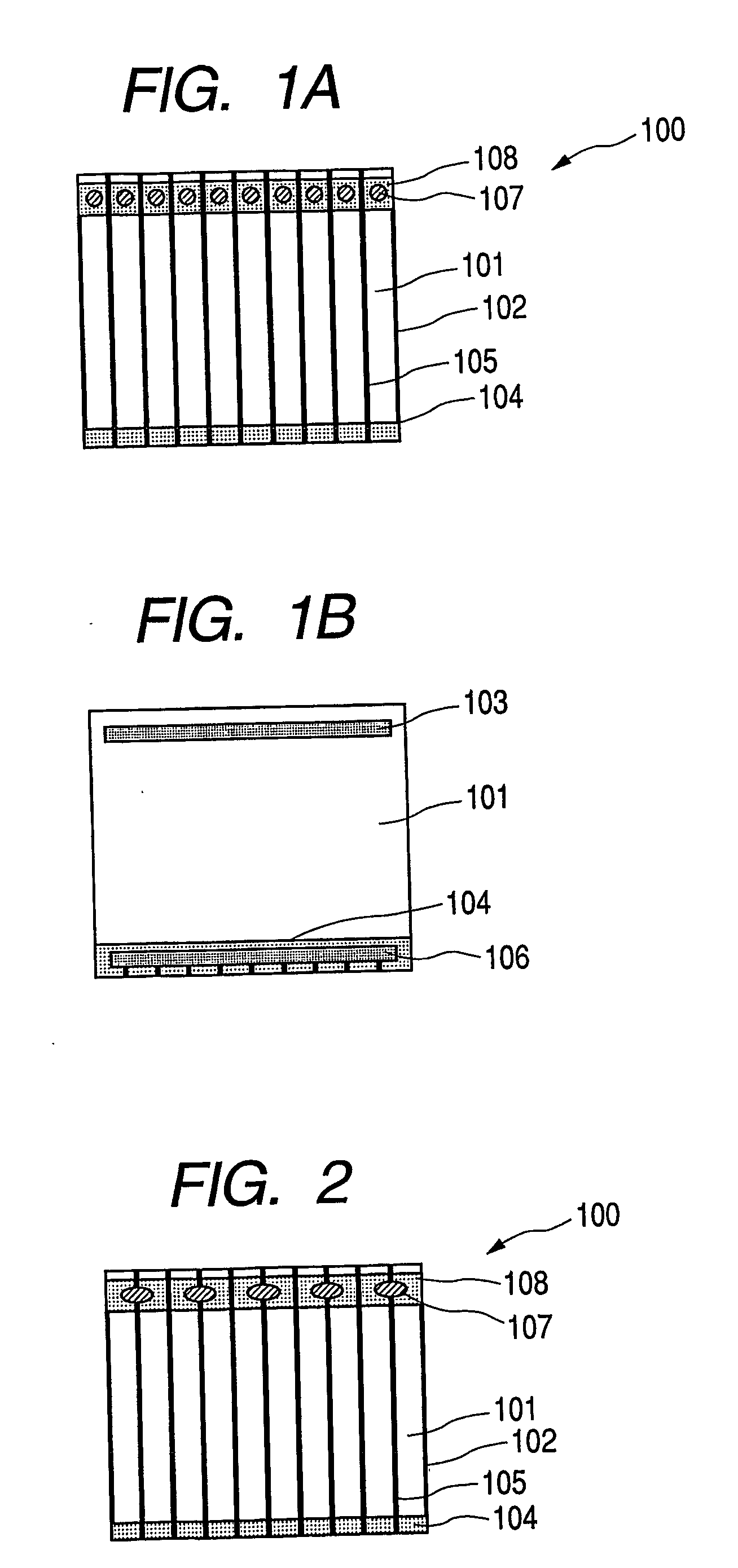
[0079]FIGS. 1A and 1B are schematic views for explaining a photovoltaic element according to Example 1 of the present invention. FIG. 1A is a schematic view of a photovoltaic element provided with current-collecting electrodes using metal wires viewed from a light-receiving surface side, and FIG. 1B is a schematic view as viewed from a non-light-receiving surface side.

[0080] In FIGS. 1A and 1B, 101 denotes a photovoltaic element plate of 200 mm×250 mm, which has three layers of a lower electrode layer, an amorphous silicon layer having a photovoltaic function and a transparent electrode layer provided on a substrate.

[0081] The photovoltaic element plate 101 is formed by sequentially depositing Al and ZnO in a thickness of several hundred nanometers respectively by sputtering right on a stainless steel sheet (substrate) having a thickness of 150 μm for supporting the whole photovoltaic element plate to thereby form a Lower electrode layer; further, sequentially depositing n-type, i...

example 2

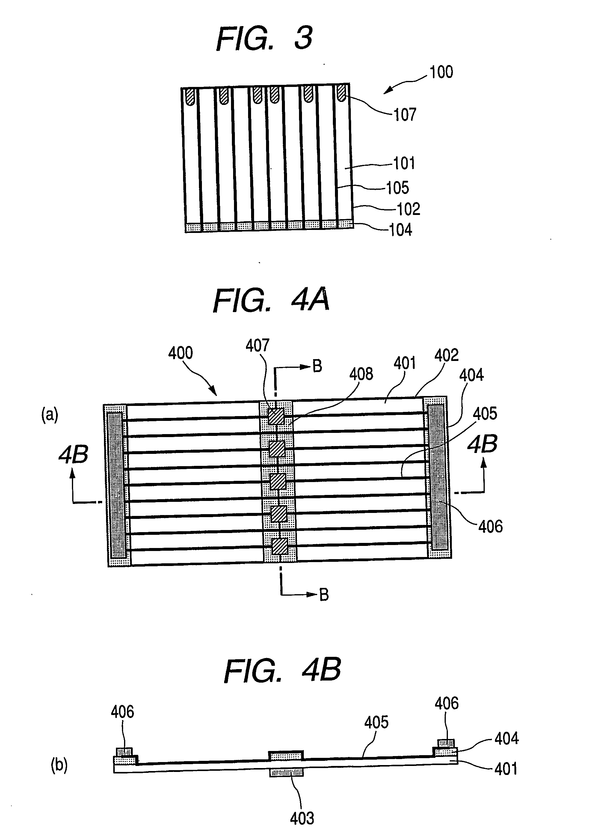
[0093]FIG. 4A to FIG. 6 are schematic views for explaining a photovoltaic element according to Example 2 of the present invention. FIG. 4A is a schematic view of the photovoltaic element viewed from a light-receiving surface side; FIG. 4B is a schematic sectional view of taken along line 4B-4B in FIG. 4A; FIG. 5A is a schematic view showing photovoltaic elements obtained by dividing the photovoltaic element of FIG. 4A along line 4B-4B in FIG. 4A; and FIG. 5B is a schematic sectional view taken along line 5B-5B in FIG. 5A.

[0094] Example 2 is directed to a photovoltaic element used in a photovoltaic generation system and differs from Example 1 in that two photovoltaic elements are previously made in one photovoltaic element, which is then divided into two to produce the photovoltaic elements, and in the shape of island-shaped transparent-electrode-layer-removed-portions.

[0095] In FIGS. 4A and 4B, 401 denotes, similarly to Example 1, a photovoltaic element plate of 200 mm×500 mm, whi...


PUM

PropertyMeasurementUnit
sizeaaaaaaaaaa
light transmittanceaaaaaaaaaa
thicknessaaaaaaaaaa

Abstract

A photovoltaic element is provided which has at least a photovoltaic layer and a transparent electrode layer deposited on a metal substrate, a portion of the transparent electrode layer being continuously removed at a peripheral part of the metal substrate, wherein an island-shaped transparent-electrode-layer-removed-portion is provided in the transparent electrode layer in a power-generating region surrounded by the removed portion of the transparent electrode layer, a rear surface side bus-bar electrode electrically connected to the metal substrate is disposed on the rear surface side of the metal substrate at the rear of the island-shaped transparent-electrode-layer-removed-portion, and the rear surface side bus-bar electrode is connected to the metal substrate at a portion corresponding to the island-shaped transparent-electrode-layer-removed-portion, and which can enhance the degree of freedom for the shape of a photovoltaic element module while ensuring the reliability of the photovoltaic element.

Description

TECHNICAL FIELD [0001] The present invention relates to a photovoltaic element used in a solar cell and a photoelectronic sensor, and particularly relates to a photovoltaic element having a rear surface side bus-bar electrode for taking out an electric power installed on a metal substrate having a semiconductor layer deposited thereon. BACKGROUND ART [0002] In recent years, a green house effect, namely, a global warming caused by an increase of CO2 becomes a subject of discussion, so that there is an increasing demand for development of a clean energy source which does not exhaust CO2. There is nuclear power generation as one of such energy sources, but it has many problems to be solved such as radioactive waste, and there is an increasing demand for a clean energy source having a higher degree of safety. [0003] Under the circumstances, a solar cell, among clean energy sources expected for the future, receives special attention in terms of cleanliness, a high degree of safety, and h...

Claims


Application Information

Patent Timeline
Patent Type & Authority Applications(United States)
IPC IPC(8): H01L31/00H01L31/04
CPCH01L31/022425H01L31/03921H01L31/0508H01L31/0201Y02E10/50
Inventor TAKEYAMA, YOSHIFUMI
Owner CANON KK
Why Eureka
Try Eureka