

Phase shift transparent structures for imaging devices
a transparent structure and imaging device technology, applied in the field of imaging devices, can solve the problems of poor image quality, noise within the circuitry, and high cost of materials, and achieve the effect of reducing the amount of cross-talk and reducing the noise within the pixel cell
- Summary
- Abstract
- Description
- Claims
- Application Information
AI Technical Summary
Benefits of technology
Problems solved by technology
Method used
Image

Examples
Embodiment Construction
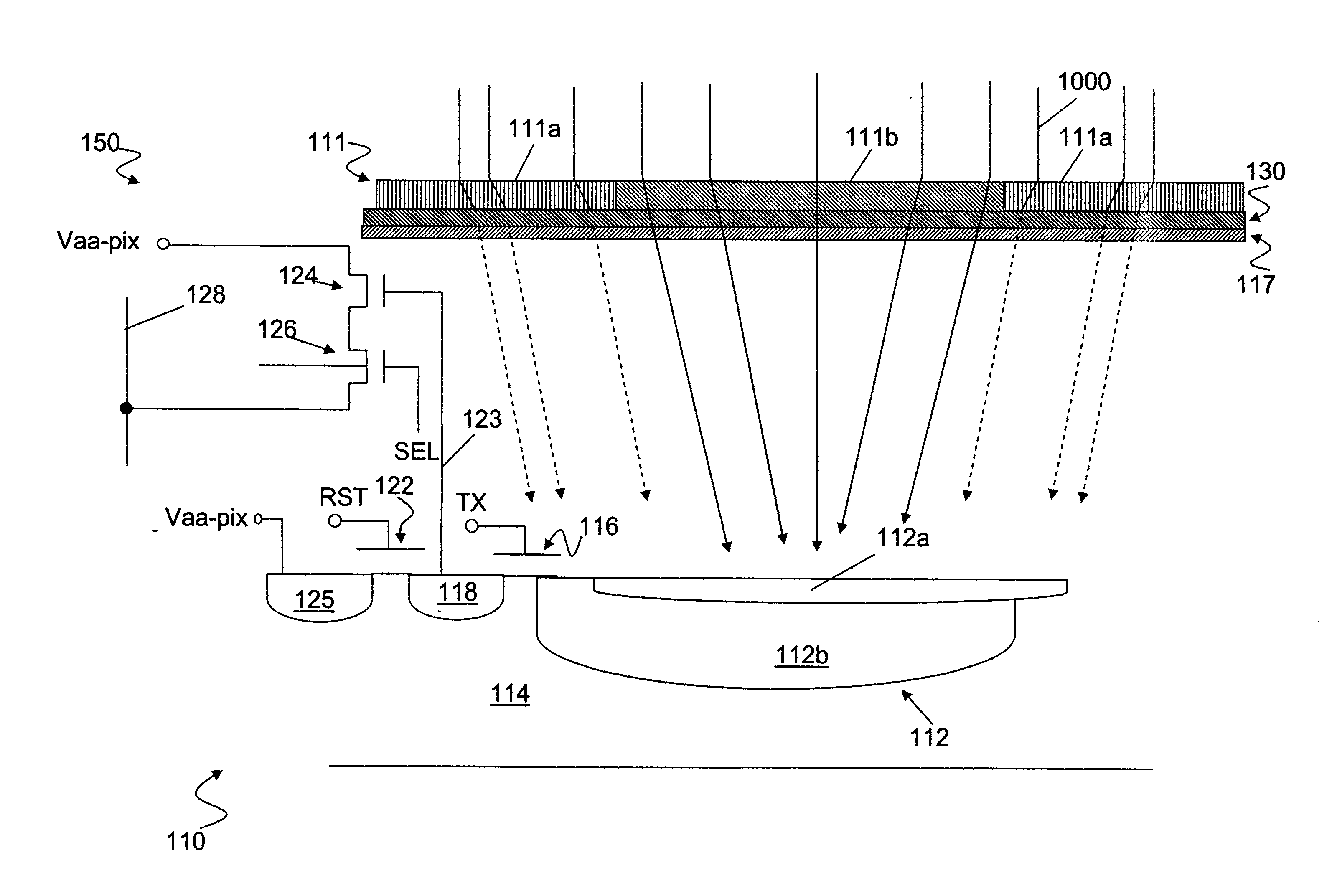
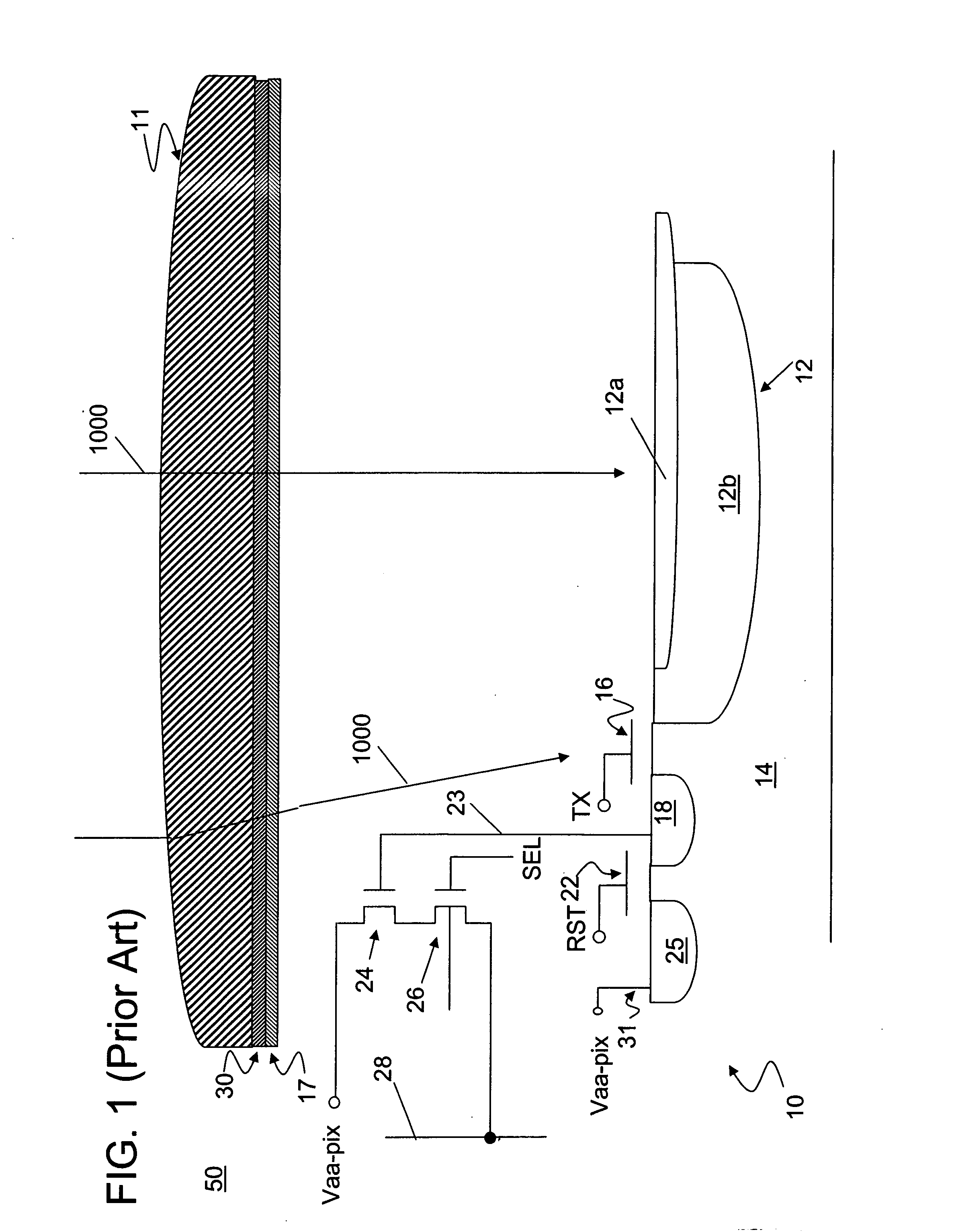
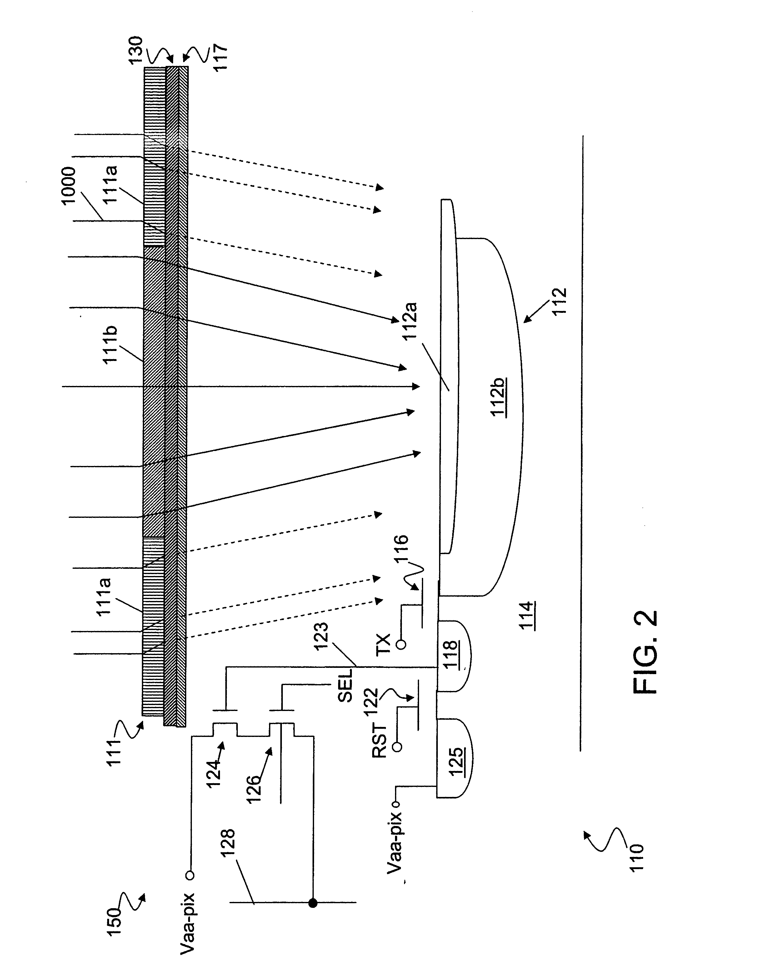
[0024] As used herein, the terms “semiconductor substrate” and “substrate” are to be understood to include any semiconductor-based structure. The semiconductor structure should be understood to include silicon, silicon-on-insulator (SOI), silicon-on-sapphire (SOS), silicon-germanium, doped and undoped semiconductors, epitaxial layers of silicon supported by a base semiconductor foundation, and other semiconductor structures. The semiconductor need not be silicon-based. The semiconductor could be germanium or gallium arsenide. When reference is made to the semiconductor substrate in the following description, previous process steps may have been utilized to form regions or junctions in or over the base semiconductor or foundation.
[0025] The term “pixel cell,” as used herein, refers to a photo-element unit cell containing a photosensor for converting photons to an electrical signal. For purposes of illustration, a single representative pixel and its manner of formation may be illustr...
PUM
 Abstract
Description
Claims
Application Information