Method of forming passive electronic components on a substrate by direct write technique using shaped uniform laser beam

a laser beam and substrate technology, applied in the direction of manufacturing tools, capacitor details, capacitor manufacture, etc., can solve the problems of unfavorable affecting the dimensional precision quality of the array, and achieve the effect of sufficient straightness, accuracy, and dimensional precision

Inactive Publication Date: 2006-11-23
ELECTRO SCI IND INC
View PDF4 Cites 18 Cited by
  • Summary
  • Abstract
  • Description
  • Claims
  • Application Information

AI Technical Summary

Benefits of technology

[0014] An object of the present invention is, therefore, to provide a method that implements a direct write laser-based technique to form an array of dimensionally precise resistive or conductive material regions whose resistive or conductive material side and end margins have sufficient straightness, accuracy, and dimensional precision to permit their use as next-generation, miniature passive electronic components.
[0016] Preferred embodiments of the method improve the dimensional precision of the opposed side and end margins by aligning with the patterned array-carrying major surface a laser beam that has a sufficient spot size and energy distribution to remove selected portions of the resistive or conductive material. The major surface carrying the resistive or conductive material and the laser beam are moved relative to each other such that the laser beam ablates, or otherwise removes, the resistive or conductive material that forms the ragged edges of the side and end margins. Thus preferred embodiments of the method form an array of multiple, mutually spaced-apart resistive or conductive material regions whose side and end margins have improved dimensional precision.
[0020] A preferred method of improving the dimensional precision of the opposed side and end margins of the regions of resistive material entails aligning a laser beam with the major surface that carries the array of resistive material regions whose dimensional precision will be improved. The laser beam has a spot size and an energy distribution sufficient to remove selected portions of the resistive material. The major surface carrying the resistive material regions whose dimensional precision will be improved and the laser beam are moved relative to each other such that the laser beam ablates, or otherwise removes, the ragged edges from the side and end margins of the resistive material regions. Thus preferred embodiments of the method form an array of multiple, mutually spaced-apart resistors whose resistive material regions have side and end margins exhibiting improved dimensional precision.
[0021] In preferred embodiments relating to the formation of an array of discrete capacitors, the substrate is an unfired “green” ceramic material on which is formed an array of conductive material regions having opposed side margins and opposed end margins. The array of conductive material regions may, for example, be formed by screen-printing an electrically conductive metallic ink onto the substrate. Each side and end margin includes ragged edges that undesirably affect the dimensional precision of the array. A preferred method of improving the dimensional precision of the opposed side and end margins entails aligning the substrate and a laser beam having a spot size and an energy distribution sufficient to remove selected portions of the screen-printable electrically conductive metallic ink. The substrate layer and the laser beam are then moved relative to each other such that the laser beam ablates, or otherwise removes, the ragged edges from the side and end margins of the conductive material regions. Thus preferred embodiments of the method form a patterned array of multiple, mutually spaced-apart conductive material regions whose side and end margins exhibit improved dimensional precision.
[0022] Multiple layers of ceramic material carrying a dimensionally precise array of conductive material regions may be stacked to form a substrate of discrete multi-layer chip capacitors (MLCCs) or a multiplicity of capacitor arrays. The multiple layers of ceramic material are preferably stacked such that the conductive material regions on adjacent layers of ceramic material are spatially aligned. In a preferred embodiment, the spatial alignment of adjacent layers of ceramic material is facilitated by the formation of alignment holes in each ceramic layer.

Problems solved by technology

Each of the end and side margins includes ragged edges that undesirably affect a dimensional precision quality of the array.

Method used


Image

  • Method of forming passive electronic components on a substrate by direct write technique using shaped uniform laser beam
  • Method of forming passive electronic components on a substrate by direct write technique using shaped uniform laser beam
  • Method of forming passive electronic components on a substrate by direct write technique using shaped uniform laser beam

Examples


Embodiment Construction

[0035] Embodiments of the present invention construct arrays of passive electronic components, such as resistors and capacitors. The term “substrate” used in connection with passive electronic components herein refers to single layer structures as well as consolidated stack, multilayer, and laminated multi-layer structures.

[0036] Exemplary preferred embodiments of the present invention are described first with reference to the formation of an array of discrete chip resistors and then with reference to the formation of a substrate layer on which is formed an array of conductive material regions.

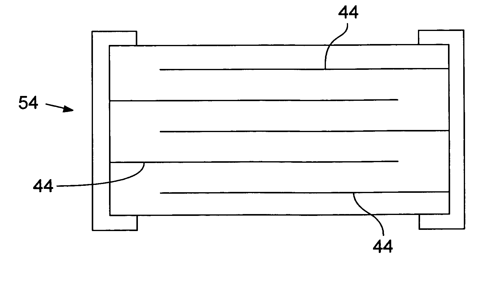
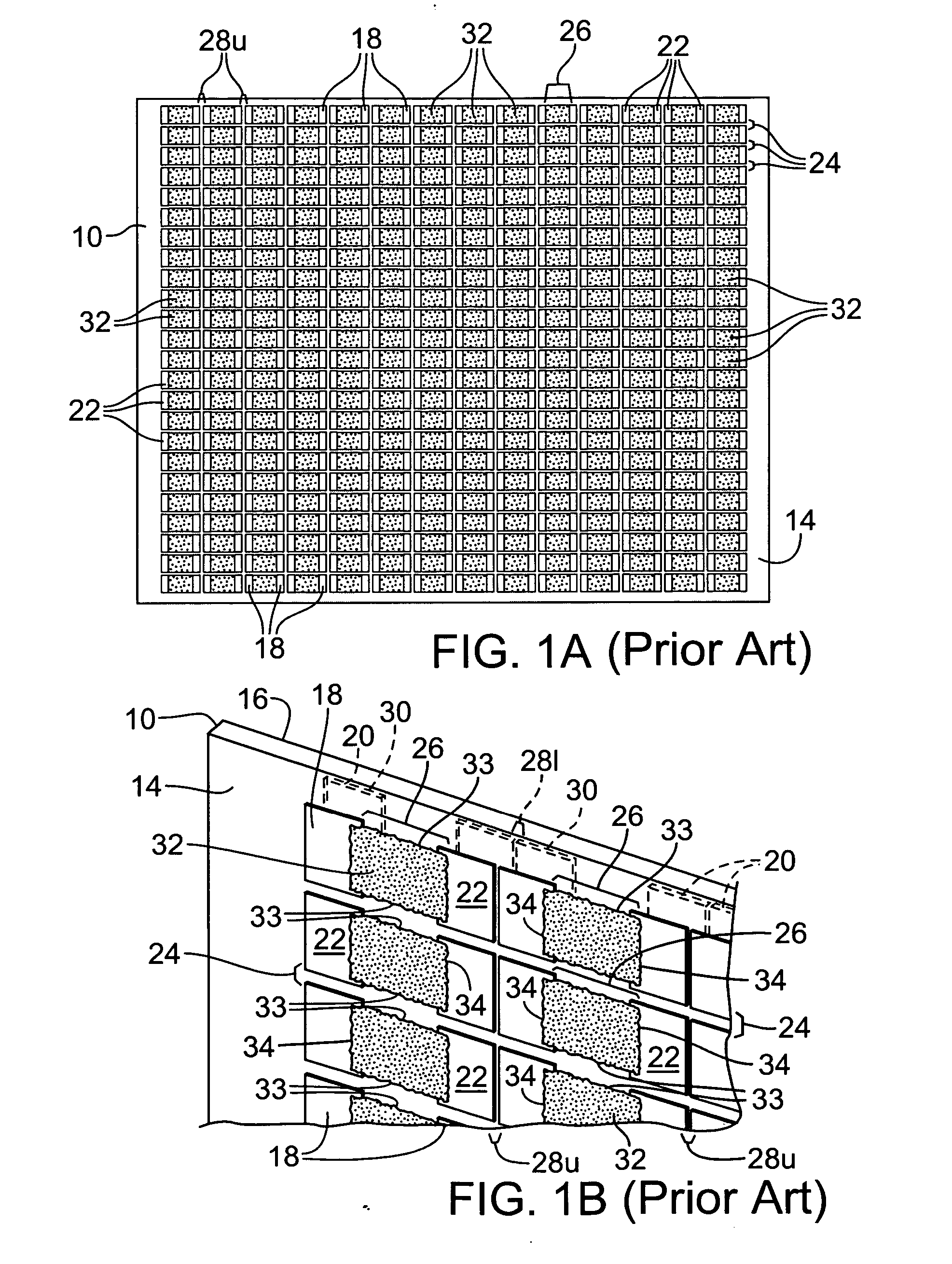
[0037] With respect to the formation of chip resistors 52, substrate 10 is preferably a fired ceramic material of 96% alumina for thick film resistors. A preferred method of forming an array of resistive material regions 32 and electrical conductor lines 18 and 20 on substrate 10 entails coating first and second major surfaces 14 and 16 of ceramic substrate 10 with an electrically conductive...


PUM

PropertyMeasurementUnit
wavelengthaaaaaaaaaa

Abstract

A method of using a laser to achieve direct patterning of resistive or electrically conductive materials in the fabrication of miniature electronic components entails aligning with a patterned array-carrying major surface a laser beam that has a sufficient spot size and energy distribution to remove selected portions of resistive or conductive material that has been applied to the substrate. The major surface carrying the resistive or conductive material and the laser beam are moved relative to each other such that the laser beam ablates, or otherwise removes, selected portions of the resistive or conductive material. Thus preferred embodiments of the method form an array of multiple, mutually spaced-apart resistive or conductive material regions whose side and end margins have improved dimensional precision.

Description

RELATED APPLICATION [0001] This application claims benefit of U.S. Provisional Patent Application No. 60 / 683,267, filed May 20, 2005.TECHNICAL FIELD [0002] The present invention relates to the efficient and accurate formation of next-generation, miniature passive electronic components and, more particularly, to a method of forming an array of spaced-apart, dimensionally precise resistive or electrically conductive material regions on a substrate. BACKGROUND INFORMATION [0003] Miniature passive electronic circuit components are conventionally fabricated in an array on a substrate. Exemplary types of passive electronic components of interest with regard to the present invention are resistors and capacitors. FIGS. 1A and 1B show an array of resistors in which a substrate 10 includes a first (or upper) major surface 14 and a second (or lower) major surface 16 carrying, respectively, first spaced-apart segmented electrical conductor lines 18 and second spaced-apart segmented electrical c...

Claims


Application Information

Patent Timeline
Patent Type & Authority Applications(United States)
IPC IPC(8): H01C10/00
CPCB23K26/408H01C7/18H01C17/006H01C17/242H01G13/006H01G4/30H01G4/33H01G13/00H01G4/255B23K26/40B23K2103/52
Inventor SWENSON, EDWARD J.HOWE, DOUGLAS B.JOHNSON, STEPHEN R.GARCIA, DOUGLAS J.
Owner ELECTRO SCI IND INC
Why Eureka
Try Eureka