Method of detachable direct bonding at low temperatures

a technology of direct bonding and detachable components, which is applied in the direction of basic electric elements, semiconductor/solid-state device manufacturing, electric devices, etc., can solve the problems of low yield, low thickness uniformity of the remaining layer, and difficult optimization of the process design needed to produce different functions on the same chip of integrated materials

Active Publication Date: 2006-11-23
INVENSAS BONDING TECH INC
View PDF63 Cites 99 Cited by
  • Summary
  • Abstract
  • Description
  • Claims
  • Application Information

AI Technical Summary

Problems solved by technology

Design of processes needed to produce different functions on the same chip of integrated materials can be difficult and hard to optimize.
Also, resultant SOC chips may get too large, leading to a low yield.
However, these methods are time consuming, environmentally unfriendly and result in a low thickness uniformity of the remaining layer.
These methods have drawbacks.
In water-enhanced de-bonding, the bonding energy of the bonded wafers has to be very low (˜100 mJ / m2) and therefore, is not sufficient for the layer transfer process steps.
Water or solvent-de-bonding also relies on the lateral reaction between the water or solvent and the adhesive bonding layer at the bonding interface is time consuming and limits the size of the bonded pairs.
For the latter, wax bonding has similar problems as in water-soluble bonding.
For the former, Apiezon wax is not strong enough for processes in a layer transfer procedure.
Hence, prior art techniques for bonding and release present numerous drawbacks and disadvantages.

Method used


Image

  • Method of detachable direct bonding at low temperatures
  • Method of detachable direct bonding at low temperatures
  • Method of detachable direct bonding at low temperatures

Examples


first example

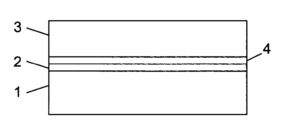
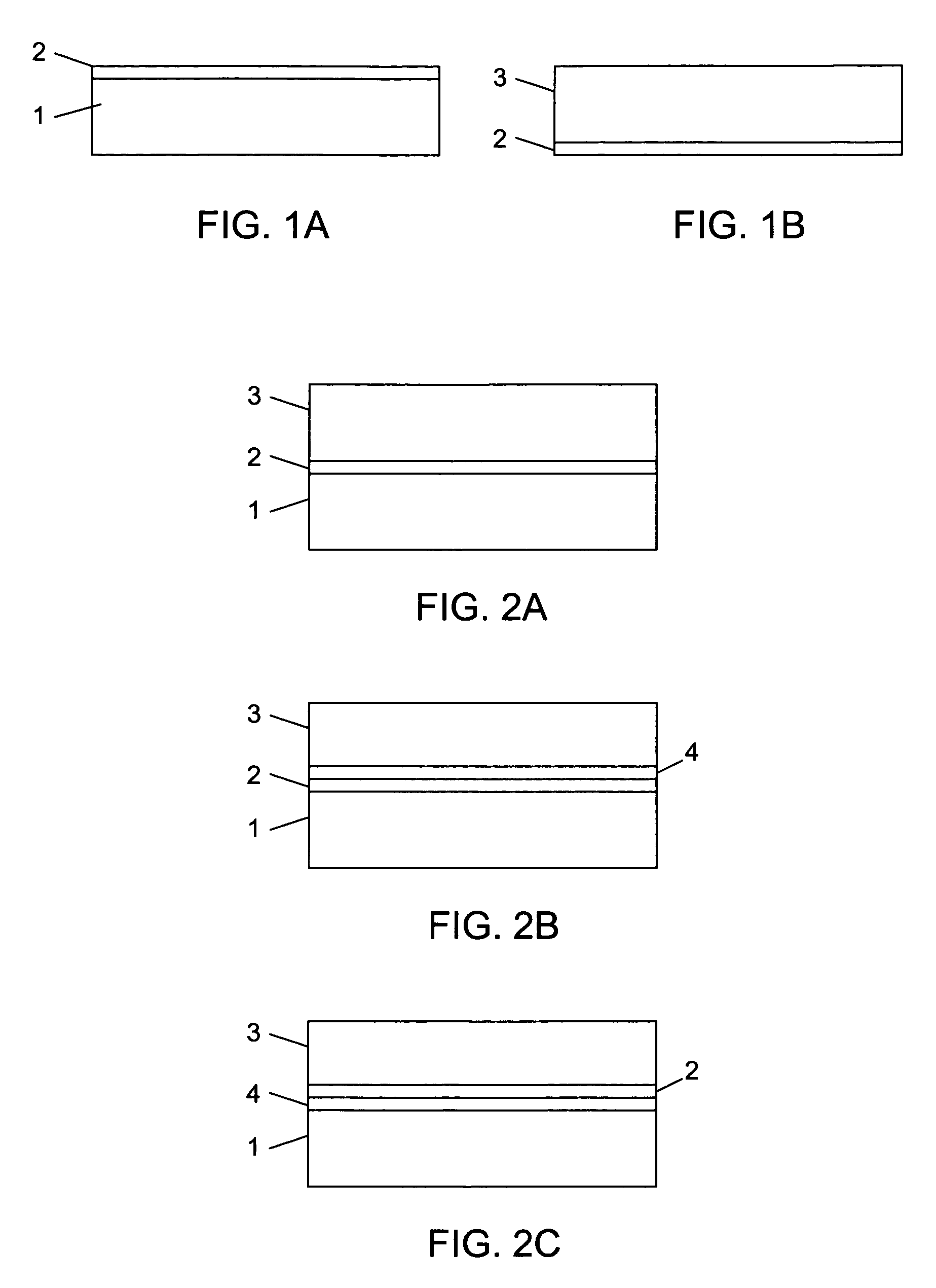
[0059] An example of the first embodiment will now be described. An intrinsic amorphous silicon (a-Si:H) layer with a thickness of about 0.7 μm and ˜16 at. % hydrogen concentration was deposited by PECVD at 190° C. on a silicon handle wafer. To enhance the adhesion between the a-Si:H and the silicon wafer, a thin silicon nitride layer (100-1000 Å) was deposited on the silicon handle wafer surface prior to a-Si:H deposition. Removal of native oxide from the silicon surface by Ar or other gas plasma sputtering before a-Si:H layer deposition will also work. The root mean square (RMS) micro-roughness of the surfaces of the as-deposited a-Si:H layer was around 15 Å, and was smoothed by performing CMP on the deposited a-Si:H layer with a soft pad to produce an RMS surface roughness of ˜1 Å. After cleaning and activation by the processes described above, the a-Si:H layer covered Si wafers were direct-bonded at about room temperature to a silicon device wafer having a planarized PECVD oxide...

second example

[0062] In a second example, a PECVD a-Si:H layer was deposited on a 300 Å SiN covered silicon handle wafer at 150° C. and doped with boron. The a-Si:H layer is 0.7 μm thick, contains ˜20 at. % hydrogen, and is in situ doped with boron to a concentration of 1×1020 cm−3. Other doping methods may be used. Due to the release of hydrogen from the silicon hydrogen complexes, surface bubbles start to generate at temperature of ˜160° C. with low density about 20 / cm2. It is known that even at room temperature B (and other group III elements) can be strongly passivated by H resulting in formation of B—H complexes. The B—H complexes dissociate at temperatures as low as 160° C. in silicon. Moreover, the Si—H bond appears to be weakened by the presence of B next to it. Planarized PECVD oxide covered Si device wafers that are fully processed and were tested were used as a matching wafer (i.e., wafer 3 in FIG. 2). The bonding energy of the room temperature bonded pair of handle wafer 1 / amorphous s...


PUM

PropertyMeasurementUnit
temperatureaaaaaaaaaa

Abstract

A method for detachable bonding that forms an amorphous silicon layer, or a silicon oxide layer with a high hydrogen content, on an element such as a carrier substrate. A second element, such as a substrate, is bonded to the amorphous silicon layer or silicon oxide layer, and the second element may then have a portion removed. A third element, such as a host or carrier substrate, is bonded to the second element or to the remaining portion of the second element to form a bonded structure. The bonded structure is then heated to cause the first element to detach from the bonded structure.

Description

CROSS REFERENCE TO RELATED APPLICATIONS [0001] This application is related to U.S. application Ser. No. 10 / 505,283 filed on Feb. 16, 2000, entitled “Method for Low Temperature Bonding and Bonded Structure,” the entire contents of which are incorporated herein by reference.DISCUSSION OF THE BACKGROUND [0002] 1. Field of the Invention [0003] This invention relates to a method of detachable direct bonding at low temperatures used for thin wafer or die layer transfer and the application of such techniques in materials, devices, and 3-D (three-dimensional) device integration. [0004] 2. Background of the Invention [0005] As the scaling limits of the conventional bulk silicon device are approaching, there is a strong demand to monolithically combine a variety of materials to form integrated materials for integrated circuits (ICs) with enhanced performances. For system-on-a chip (SOC) preparation, a variety of functions are required on a chip. Many functions are usually best made from their...

Claims


Application Information

Patent Timeline
Patent Type & Authority Applications(United States)
IPC IPC(8): H01L21/30
CPCH01L21/76254H01L21/2007
Inventor TONG, QIN-YIFOUNTAIN, GAIUS GILLMAN JR.
Owner INVENSAS BONDING TECH INC
Why Eureka
Try Eureka