In-situ profile measurement in an electroplating process

a technology of in-situ profile measurement and electroplating process, which is applied in the direction of electrical/magnetic thickness measurement, instruments, transportation and packaging, etc., can solve the problems of inability to accurately measure the current distribution of the plating cell, the feature on some portions of the substrate may be undesired or even filled up, and the thin conductive seed layer formed on the substrate is generally very thin

Inactive Publication Date: 2006-11-30
APPLIED MATERIALS INC
View PDF32 Cites 34 Cited by
  • Summary
  • Abstract
  • Description
  • Claims
  • Application Information

AI Technical Summary

Benefits of technology

[0015] The details of one or more implementations are set forth in the accompanying drawings and the descript

Problems solved by technology

However, with conventional ECP processes and systems, the conductive seed layer formed on the substrate is generally very thin, and as such, is highly resistive.
This phenomenon is generally known as the “terminal effect”, and is an undesirable characteristic associated with conventional plating systems.
Another challenge in an electrochemical proc

Method used


Image

  • In-situ profile measurement in an electroplating process
  • In-situ profile measurement in an electroplating process
  • In-situ profile measurement in an electroplating process

Examples


Embodiment Construction

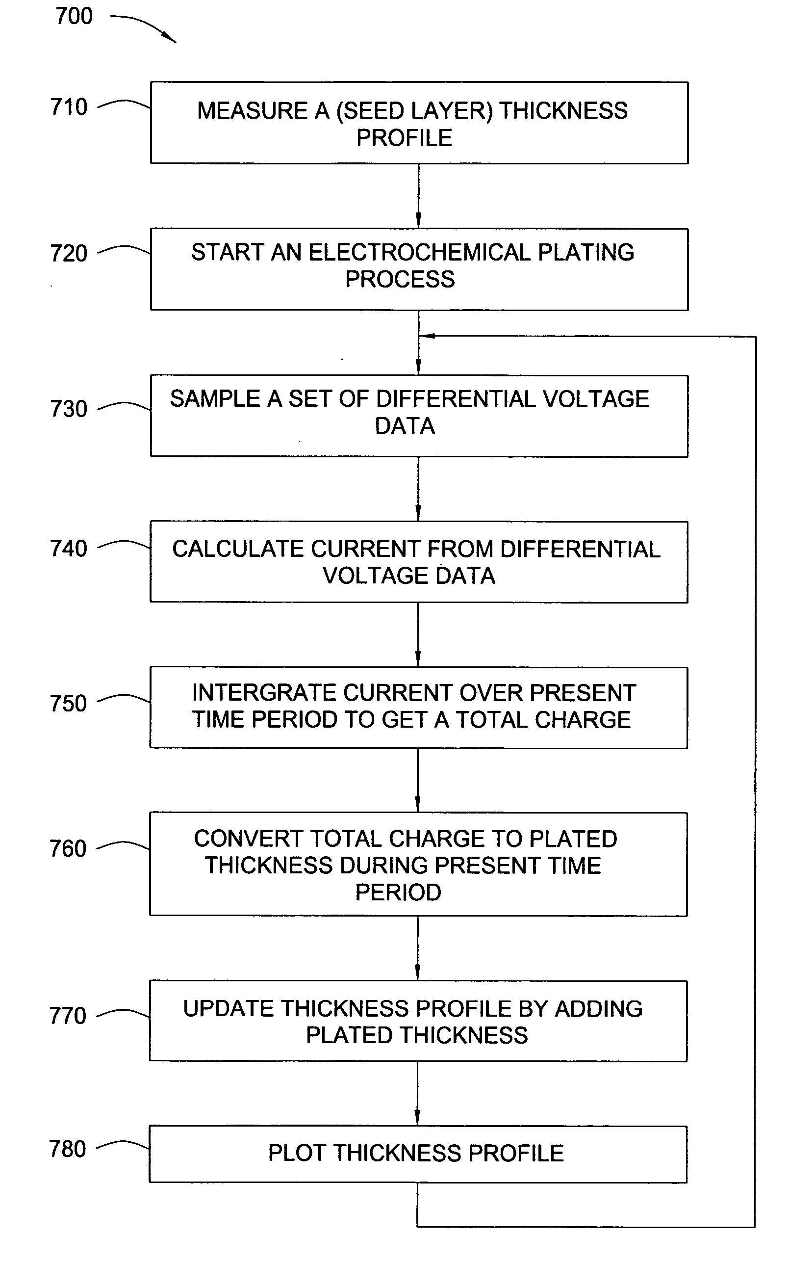
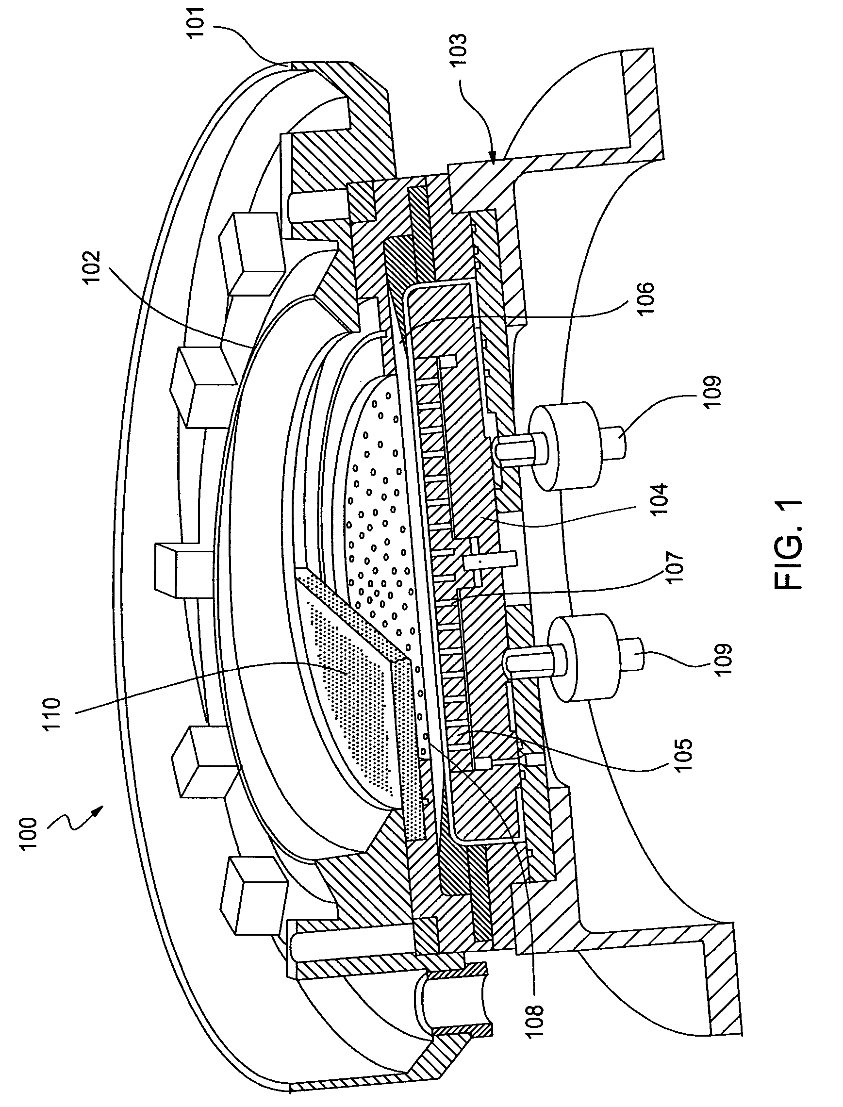
[0040] The present invention generally provides an electrochemical plating cell configured to plate a metal onto a semiconductor substrate. The plating cell of the invention generally includes a fluid volume cell, a contact ring, an anode and array of sensors disposed in the fluid volume. The array of sensors positioned in the fluid volume are configured to measure cell current distributions during plating. A thickness profile of plated metal can be generated from the cell current distributions using a method provided by the present invention.

[0041]FIG. 1 illustrates a schematic view of an exemplary plating cell 100. The plating cell 100 generally includes an outer basin 101 and an inner basin 102 positioned within the outer basin 101. The inner basin 102 is generally configured to contain a plating solution that is used to plate a metal, e.g., copper, onto a substrate during an electrochemical plating process. During the plating process, the plating solution is generally continuou...


PUM


Abstract

A method and apparatus for measuring differential voltages in an electrolyte of an electrochemical plating cell. Current densities are calculated from the measured differential voltages and correlated to thickness values of plated materials. A real time thickness profile may be generated from the thickness values.

Description

BACKGROUND OF THE INVENTION [0001] 1. Field of the Invention [0002] Embodiments of the invention generally relate to measuring spatial plating cell current distribution represented by measuring the differential voltages inside an electrochemical plating cell in-Situ. [0003] 2. Description of the Related Art [0004] In semiconductor processing, electrochemical plating (ECP) is generally the preferred technique for filling features formed onto substrates with a conductive material. A typical ECP process generally includes immersing a substrate into an electrolyte solution that is rich in ions of the conductive material (generally copper), and then applying an electrical bias between a conductive seed layer formed on the surface of the substrate and an anode positioned in the electrolyte solution. The application of the electrical bias between the seed layer and the anode facilitates an electrochemical reaction that causes the ions of the conductive material to plate onto the seed layer...

Claims


Application Information

Patent Timeline
IPC IPC(8): C25D21/12
CPCC25D21/12G01B7/06G01B7/287Y10T428/24802C25D7/123C25D17/001H01L21/67253C25D5/60
Inventor BIRANG, MANOOCHERKOVARSKY, NICOLAY Y.DONOSO, BERNARDO
Owner APPLIED MATERIALS INC
Why Eureka
Try Eureka