High power light emitting diode package and fabrication method thereof

Inactive Publication Date: 2006-11-30
SAMSUNG ELECTRONICS CO LTD
View PDF4 Cites 71 Cited by
  • Summary
  • Abstract
  • Description
  • Claims
  • Application Information

AI Technical Summary

Benefits of technology

[0018] The present invention has been made to solve the foregoing problems of the prior art and it is therefore an object of the present invention to provide a high power LED package in which t

Problems solved by technology

Thus, with high level of power consumption, the LED typically adopts a heat conducting structure to prevent the semiconductor device and the package itself from being damaged from the heat generated during the emission of light.
Therefore, the assembly structure and process is too complicated to be fully automated, lowering productivity.
In addition, the package has a large volume with too many components therein.
Still, the heat conducting structure and the

Method used


Image

  • High power light emitting diode package and fabrication method thereof
  • High power light emitting diode package and fabrication method thereof
  • High power light emitting diode package and fabrication method thereof

Examples


Example

[0076] Preferred embodiments of the present invention will now be described in detail with reference to the accompanying drawings.

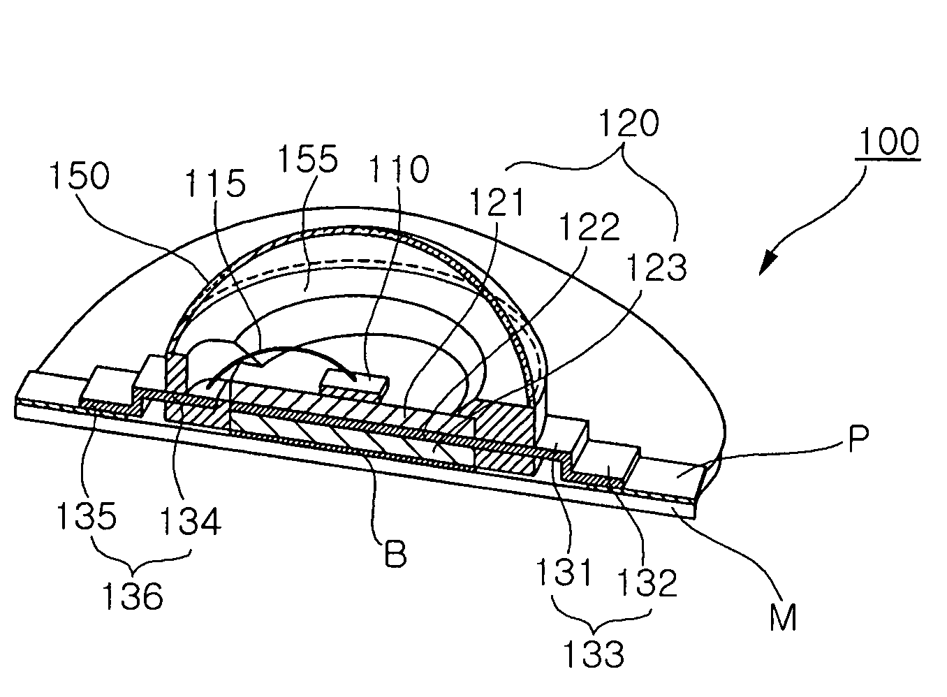
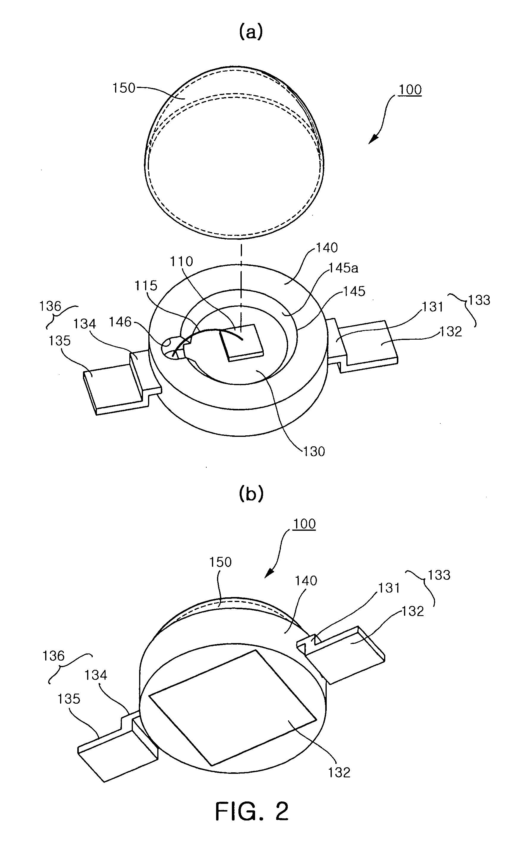
[0077] As shown in FIGS. 2(a) and (b) and FIG. 3, an LED package 100 according to the present invention including a light emitting part 110, a heat conducting part 120, a lead part 130 and a mold part 140, integrates two components into a single one, reducing the number of components, thereby simplifying the assembly process.

[0078] The light emitting part 110 is composed of at least one semiconductor device which generates a predetermined intensity of light in response to power applied and generates heat in proportion to the intensity of current applied at the same time.

[0079] Such a semiconductor device is composed of material such as GaAlAs-based material use in an active layer and a cladding layer covering the active layer, AlGain-based, AlGainP-based and AlGainPAs-based material used in red semiconductor laser devices of high-density optical discs,...


PUM


Abstract

The invention relates to a high power LED package and a fabrication method thereof. The LED package includes a light emitting part for generating light in response to power applied, a heat conducting member with the light emitting part mounted thereon, a lead part for electrically connecting the light emitting part and a board, and a mold part for integrally fixing the heat conducting member and the lead part. The heat conducting member is composed of at least two metal layers in a height direction, and the lead part includes at least one first lead extended out of the heat conducting member and at least one second lead separated from the heat conducting member. The invention allows integration of two components into a single one, reducing the number of components and simplifying the assembly process, thereby reducing the manufacturing costs.

Description

CLAIM OF PRIORITY [0001] This application claims the benefit of Korean Patent Application No. 2005-45787 filed on May 30, 2005, in the Korean Intellectual Property Office, the disclosure of which is incorporated herein by reference. BACKGROUND OF THE INVENTION [0002] 1. Field of the Invention [0003] The present invention relates to a high power Light Emitting Diode (LED) package and a fabrication method thereof. More particularly, the invention relates to a high power LED package in which a lead part is integrated with a heat conducting member into a single component to reduce the number of components constituting the package, simplifying the assembly structure and process to reduce the manufacturing costs, and a fabrication method thereof. [0004] 2. Description of the Related Art [0005] In general, a Light Emitting Diode (LED) is a semiconductor light emitting device that emits light in response to power applied, and adopts a PN junction diode composed of for example, GaAs or GaN o...

Claims


Application Information

Patent Timeline
IPC IPC(8): H01L33/00H01L33/32H01L33/44H01L33/56H01L33/58H01L33/60H01L33/62H01L33/64
CPCH01L33/60H01L33/62H01L33/641H01L33/647H01L2224/48247H01L2224/48091H01L2924/00014H01L24/97H01L2924/181H01L2924/00012
Inventor LEE, SEON GOOHAHM, HUN JOOKIM, DAE YEONSONG, YOUNG JAEPARK, YOUNG SAMSONG, CHANG HO
Owner SAMSUNG ELECTRONICS CO LTD
Why Eureka
Try Eureka