Organic thin film transistor, method of fabricating the same, and flat panel display having the organic thin film transistor

Active Publication Date: 2006-11-30
SAMSUNG DISPLAY CO LTD
View PDF12 Cites 19 Cited by
  • Summary
  • Abstract
  • Description
  • Claims
  • Application Information

AI Technical Summary

Benefits of technology

[0016] It is further an object of the present invention to provide an organic thin film transistor and a flat panel display using the same and a method of making the organic thin film transistor where the

Problems solved by technology

The organic electro-luminescence display device that uses the plastic substrate has to be manufactured by a low temperature process since the plastic substrate has very low thermal stability.
As a result, there is a leakage current prob

Method used


Image

  • Organic thin film transistor, method of fabricating the same, and flat panel display having the organic thin film transistor
  • Organic thin film transistor, method of fabricating the same, and flat panel display having the organic thin film transistor
  • Organic thin film transistor, method of fabricating the same, and flat panel display having the organic thin film transistor

Examples


first embodiment

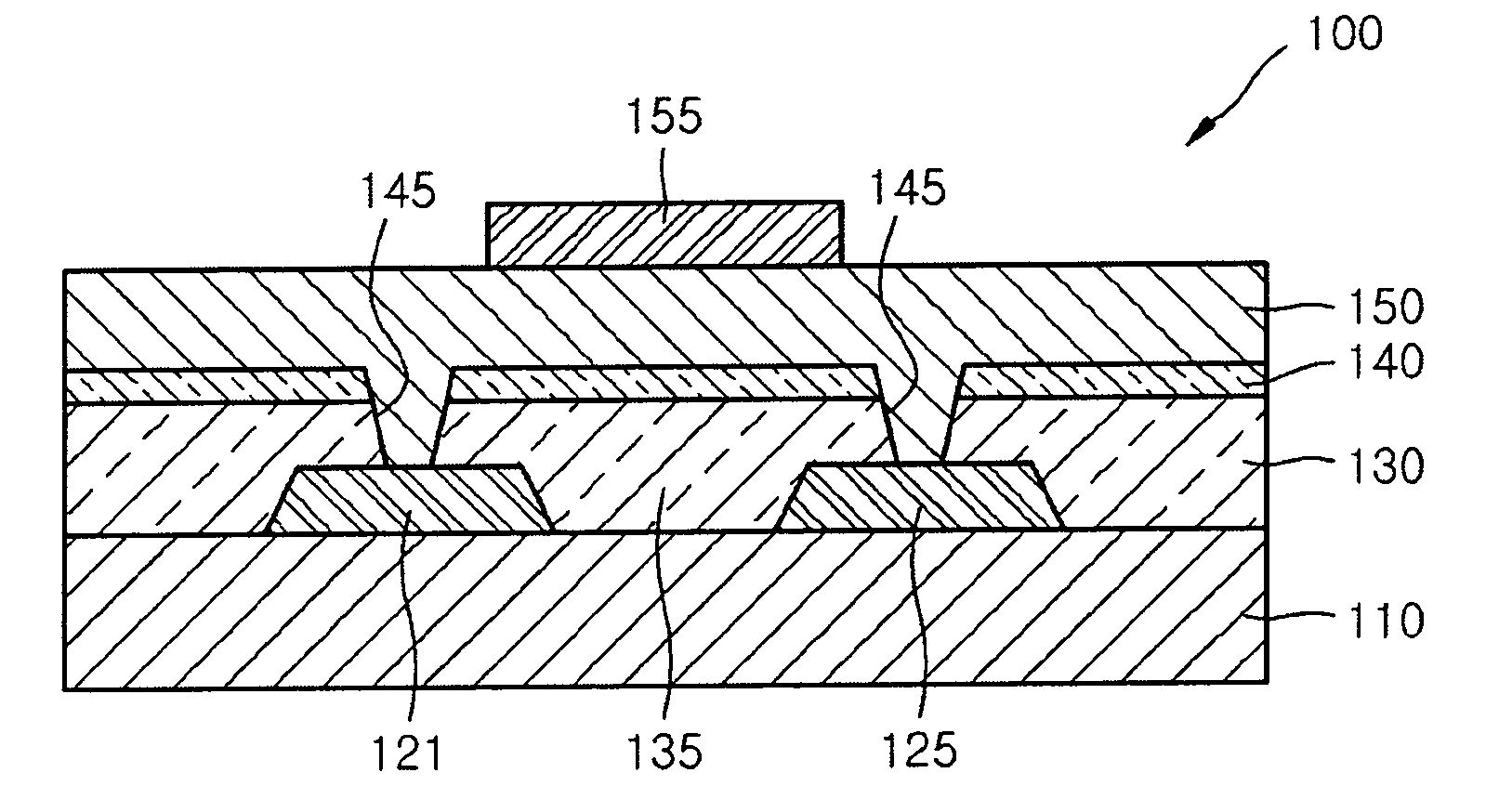
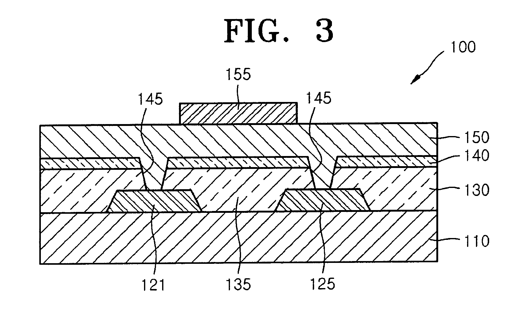
[0038] Turning now to FIG. 3, FIG. 3 is a cross-sectional view illustrating an organic thin film transistor 100 according to the present invention. The organic thin film transistor 100 of FIG. 3 is a top-gate type structure. Referring to FIG. 3, source and drain electrodes 121 and 125 are formed on a substrate 110. A semiconductor layer 130 is formed on the substrate 110 and the source and drain electrodes 121 and 125 to contact the source and drain electrodes 121 and 125, and a protective film 140 is formed on the semiconductor layer 130. A gate insulating film 150 is formed on the protective film 140. A gate electrode 155 is formed on the gate insulating film 150 to correspond to a channel region 135 of the semiconductor layer 130 disposed between the source and drain electrodes 121 and 125. The substrate 110 can be one of a glass substrate, a plastic substrate, and a metal substrate. The metal substrate can be formed of steel use stainless (SUS). The plastic substrate can include...

second embodiment

[0058] Turning now to FIG. 6, FIG. 6 is a cross-sectional view of an organic thin film transistor 200 used in a flexible organic electro-luminescence display according to the present invention. The organic thin film transistor 200 of FIG.6 is a bottom gate type structure. Referring to FIG. 6, a gate 215 is formed on a substrate 210, and a gate insulating film 220 is formed on the substrate 210 covering the gate 215. Source and drain electrodes 231 and 235 are formed on the gate insulating film 220. A semiconductor layer 240 is formed on the gate insulating film 220 to contact the source and drain electrodes 231 and 235. A protective film 250 is formed on the semiconductor layer 240.

[0059] The substrate 210 can be one of a glass substrate, a plastic substrate, and a metal substrate. The semiconductor layer 240 is an organic semiconductor layer. The gate insulating film 220 can have one or more layers, each layer being either an organic insulating film, an inorganic insulating film an...

third embodiment

[0062] Turning now to FIG. 7, FIG. 7 is a cross-sectional view of an organic thin film transistor 300 according to the present invention. The organic thin film transistor 300 is a top gate type structure similar to that of transistor 100 of FIG. 3. Referring to FIG. 7, source and drain electrodes 321 and 325 are formed on a substrate 310, and a semiconductor layer 335 is formed on the substrate 310 over and in contact with the source and drain electrodes 321 and 325 as well as between the source and drain electrodes 321 and 325. A protective film 345 is formed on the semiconductor layer 335. The protective film 345 and the semiconductor layer 335 are patterned to form the channel region. A gate insulating film 350 is formed on the resultant structure, and a gate electrode 355 is formed on the gate insulating film 350.

[0063] The substrate 310 can be one of a glass substrate, a plastic substrate or a metal substrate. The metal substrate can be formed of steel use stainless (SUS). The ...


PUM

PropertyMeasurementUnit
Thicknessaaaaaaaaaa
Dielectric constantaaaaaaaaaa

Abstract

An organic thin film transistor that prevents the surface of an organic semiconductor layer from being damaged and reduces turn-off current, a method of fabricating the same, and an organic light-emitting device incorporating the organic thin film transistor. The organic thin film transistor includes a substrate, source and drain electrodes arranged on the substrate, a semiconductor layer contacting the source and drain electrodes and comprising a channel region, a protective film arranged on the semiconductor layer and having a same pattern as the semiconductor layer, the protective film comprising a laser-absorbing material, a gate insulating film arranged between the gate and the source and drain electrodes, a gate electrode arranged on the gate insulating film and a separation pattern arranged within the semiconductor layer and within the protective film, the separation pattern adapted to define the channel region of the semiconductor layer.

Description

CLAIM OF PRIORITY [0001] This application makes reference to, incorporates the same herein, and claims all benefits accruing under 35 U.S.C. §119 from an application earlier filed in the Korean Intellectual Property Office on 24 May 2005 and there duly assigned Serial No. 10-2005-0043702. BACKGROUND OF THE INVENTION [0002] 1. Field of the Invention [0003] The present invention relates to a thin film transistor for flat panel displays, and more particularly, to an organic thin film transistor that prevents the surface of an organic semiconductor layer from being damaged, and a flat panel display having the same. [0004] 2. Description of the Related Art [0005] Studies on organic thin film transistors (OTFTS) for use in next generation display devices have been actively performed. OTFTs use an organic film instead of a silicon film as a semiconductor layer, and are classified into low molecule organic thin film transistors such as using oligothiophene and pentacene, and polymer organic...

Claims


Application Information

Patent Timeline
IPC IPC(8): H01L27/12
CPCH01L27/283H01L27/3274H01L51/0545H01L51/0036H01L51/0541H01L51/0017H10K19/10H10K59/125H10K71/231H10K85/113H10K10/464H10K10/466
Inventor AHN, TAEKSUH, MIN-CHULMO, YEON-GON
Owner SAMSUNG DISPLAY CO LTD
Why Eureka
Try Eureka