Optical method and device for texture quantification of photovoltaic cells

a technology of photovoltaic cells and optical methods, applied in measurement devices, instruments, scientific instruments, etc., can solve the problems of high cost of crystalline materials, damage to analyzed areas, and difficulty in quality control systems of cell texture, etc., and achieve the effect of less intensity

Inactive Publication Date: 2006-11-30
CONSEJO SUPERIOR DE INVESTIGACIONES CIENTIFICAS (CSIC)
View PDF3 Cites 12 Cited by
  • Summary
  • Abstract
  • Description
  • Claims
  • Application Information

AI Technical Summary

Problems solved by technology

Due to the high cost of crystalline materials, industrial production of photovoltaic cell technology is focused on silicon substrates (Si), although several crystalline quality grades are used.
Aside from the cost incurred in the utilization of these techniques, their adaptations to the industry as a quality control system of the cell's texture present certain difficulties.
The scanning electron microscopy (SEM) requires a low pressure environment around the cell to work and the analyzed area may sustain damages due to the incidence of the electron beam.
Also, the time required to perform the analysis considerably exceeds the speed of processing required for the production process.
The profilometers, on the other hand, either work in contact mode, which may scratch the cell, or in optical mode that, while without contact, is developed to work on flat surfaces and do not adapt well to rugged and faceted surfaces because the reflectance is non-specular.

Method used


Image

  • Optical method and device for texture quantification of photovoltaic cells
  • Optical method and device for texture quantification of photovoltaic cells
  • Optical method and device for texture quantification of photovoltaic cells

Examples


Embodiment Construction

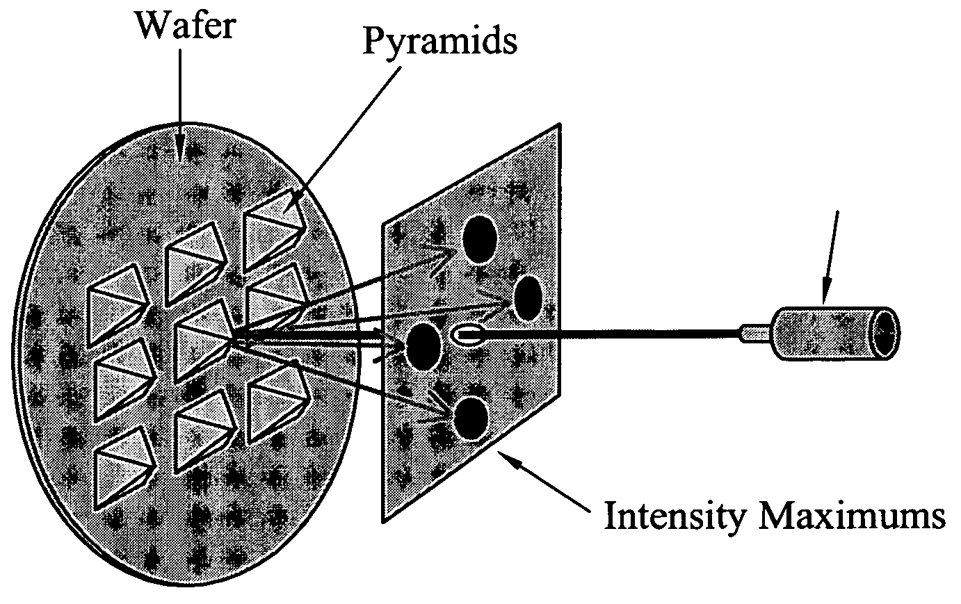
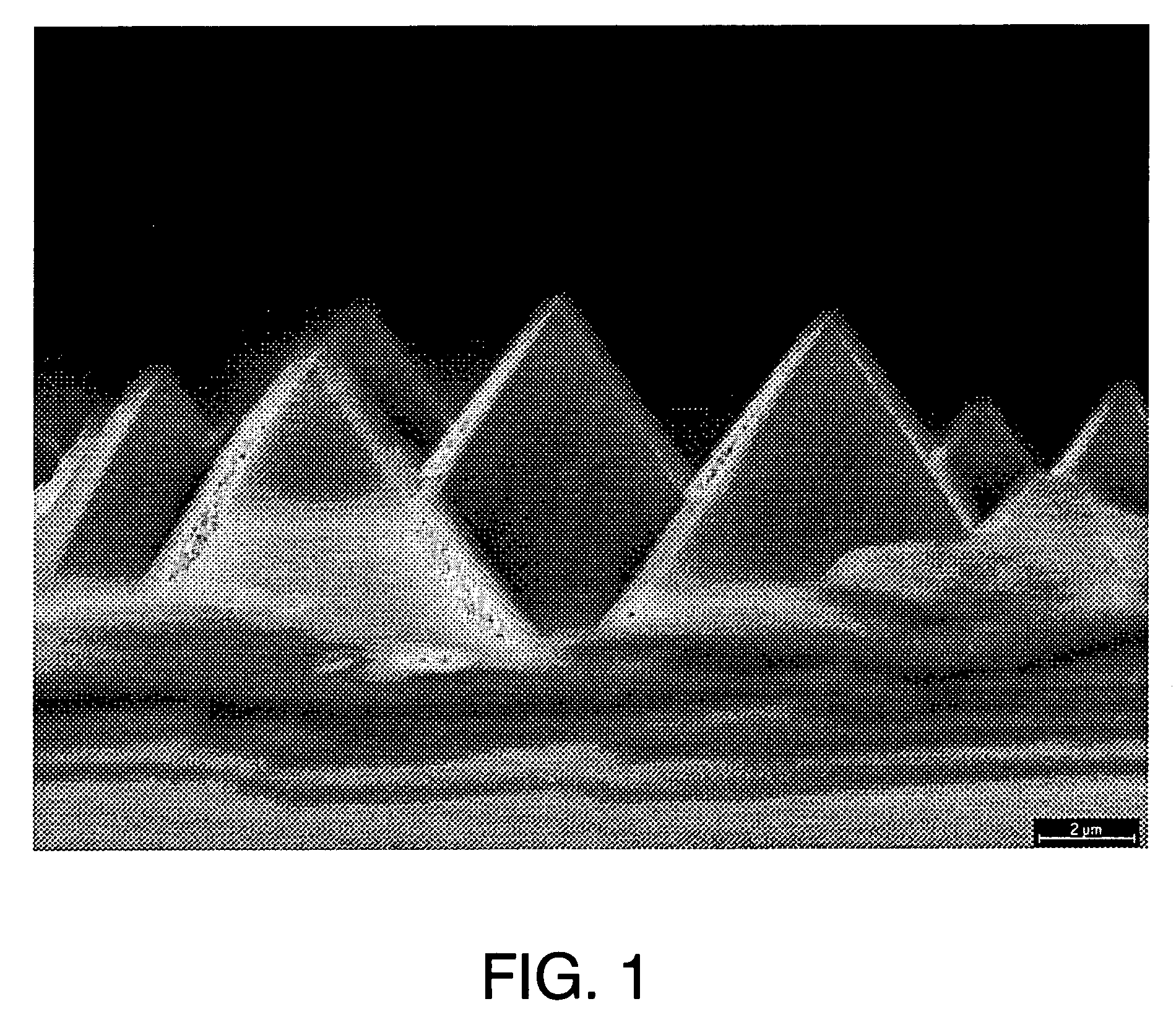
[0042] As described above, the method entails determining the pattern of reflectance associated to a textured surface (particularly those Si surfaces that have been subject to chemical etching to attain pyramidal shapes) that is originated by the light of a laser beam with normal incidence. This pattern is captured on a flat screen as shown on FIG. 3a. According to the laws of reflection, the expected pattern for a surface composed of equal pyramid shapes would be composed of four points symmetrically located around the axis of the incoming beam, however, the presence of defects, non-textured areas, etc., causes an increase of the normal reflectance in detriment of the intensity associated to the texturing, which is the bases of the present method.

[0043] The geometry of the screen may be adapted to the circumstances of the design. FIGS. 3a and 3b, respectively, show some of the alternatives that include spherical or semi-spherical screens, in which the wafer is placed in the middle...


PUM

PropertyMeasurementUnit
tilt angleaaaaaaaaaa
diameteraaaaaaaaaa
aaaaaaaaaa

Abstract

The invention relates to an optical method and device for the texture quantification of photovoltaic cells. The inventive method and device are suitable for texture morphologies that are characterized by the development of geometric patterns which are correlated on the surface of the substrate supporting the photovoltaic cell. The aforementioned morphologies can be formed using different methods, including chemical attack of monocrystalline Si, with both raised and inverted pyramids. The inventive method can also be used to study other degrees of texture developed in multicrystalline Si as well as those present in polycrystalline silicon cells deposited on substrates which have been pre-textured under the aforementioned conditions. The invention can also be extended to other materials having similar texture patterns.

Description

RELATED APPLICATIONS [0001] The present application is a Continuation of co-pending PCT Application No. PCT / ES2004 / 070050, filed Jul. 14, 2004 which in turn, claims priority from Spanish Application Serial No. 200301666, filed on Jul. 15, 2003. Applicants claim the benefits of 35 U.S.C. §120 as to the PCT application and priority under 35 U.S.C. §119 as to said Spanish application, and the entire disclosures of both applications are incorporated herein by reference in their entireties.BACKGROUND OF THE INVENTION [0002] 1. Field of the Invention [0003] This invention is related to the production engineering industry, and more particularly to the sector concerned with the production of photovoltaic cells, and therefore it also has a bearing on the alternative energy sector. The invention relates to the control of the methods used for texturing the surface of monocrystalline silicon, although it is also applicable to the textures developed on the surface of silicon and other multicryst...

Claims


Application Information

Patent Timeline
Patent Type & Authority Applications(United States)
IPC IPC(8): G01B11/30G01N21/47
CPCG01B11/30G01N2021/4735G01N21/47
Inventor ZALDO LUEZAS, CARLOS ENRIQUEALBELLA MARTIN, JOSE MARIAFORNIES GARCIA, EDUARDO
Owner CONSEJO SUPERIOR DE INVESTIGACIONES CIENTIFICAS (CSIC)
Why Eureka
Try Eureka