Semiconductor device and method for manufacturing the same

a semiconductor device and semiconductor technology, applied in the direction of semiconductor devices, semiconductor/solid-state device details, radiation control devices, etc., can solve the problems of weak mounting intensity, different sensing results of each light, and inability to form the connection terminal of a wiring substrate on a side face of a plastic substrate, etc., to achieve the effect of improving the reliability of mounting the semiconductor devi

Active Publication Date: 2006-11-30
SEMICON ENERGY LAB CO LTD
View PDF38 Cites 10 Cited by
  • Summary
  • Abstract
  • Description
  • Claims
  • Application Information

AI Technical Summary

Benefits of technology

[0014] In view of the foregoing, it is an object of the present invention to provide a semiconductor device having the structure that can be mounted on a wiring substrate and is formed over a thin substrate, a film-shaped substrate, or a sheet-like substrate. It is another object of the present invention to provide a manufacturing method of a semiconductor device that can enhance the reliability of mounting the semiconductor device over a wiring substrate.
[0018] As the method for bonding the substrate having insulation and the member that the conductive film is formed via a medium having anisotropic conductivity, a pressure bonding method that adds load partially is given. In this case, it is preferably to apply load to the substrate and the member, and the while adding heat or ultrasonic wave thereto. When pressure bonding is carried out while applying ultrasonic wave, vibrational energy is transmitted to a conductive particle from each of the terminal, that is, an electrode terminal and a connection terminal. As a result, friction is generated between each of the terminal and the conductive particle, and joining of each of the terminal and the conductive particle is promoted by means of energy due to the frictional heat. Therefore, joining at low temperature is possible.
[0021] It is preferable that an area of the substrate provided with the semiconductor element and an area of the interposer is approximately the same. Moreover, the area of the substrate provided with the semiconductor element may be larger than the area of the interposer. In this case, a region provided with the semiconductor element is increased. Therefore, a further integrated semiconductor device can be manufactured. In addition, the area of the interposer may be larger than the area of the substrate provided with the semiconductor element. In this case, an area to be bonded to a wiring substrate is increased, and so the stability is increased in the mounting portion.
[0022] As a result, a semiconductor device can be mounted over the wiring substrate with high reliability.
[0030] In the semiconductor device according to the present invention, the semiconductor element can be electrically connected to a connection terminal (side electrode) of the interposer, therefore, an area to be joined to the wiring substrate is increased. That is, a joining mode can be checked with eyes, in addition that mounting intensity can be raised.
[0031] Moreover, the connection of the semiconductor element and the interposer is strong because these two members are bonded in an aspect of entire surface facing each other. Moreover, the cost can be reduced because these two members are connected by means of resin. In addition, resin has high fixing strength, so the semiconductor device having high breaking strength can be manufactured.

Problems solved by technology

Therefore, in the case that the optical sensor using single crystal silicon or polysilicon senses white fluorescent light that hardly include a spectrum of an infrared region and sunlight that has a wide spectrum from an ultraviolet region to an infrared region, there is a problem that sensing result of each light is different while actual brightness is the same.
However, a connection terminal of a wiring substrate cannot be formed on a side face of a plastic substrate because of its thin thickness.
The area of the face is small, thus, there is a problem that the mounting intensity is weaker than that of a side electrode structure.
In addition, it is difficult to see a junction between an electrode terminal of the optical sensor and an electrode pat to judge whether they connect to each other surely, because a region where the wiring substrate is connected to the optical sensor is the lower part of a substrate of the optical sensor.
Moreover, a film-shaped optical sensor is hard to mount over the wiring substrate because of its flexibility.

Method used


Image

  • Semiconductor device and method for manufacturing the same
  • Semiconductor device and method for manufacturing the same
  • Semiconductor device and method for manufacturing the same

Examples


embodiment mode 1

[0042] An optical sensor of the present invention is described with reference to FIGS. 1A and 1B.

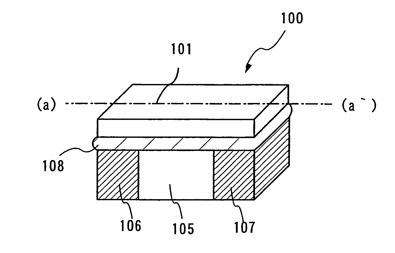
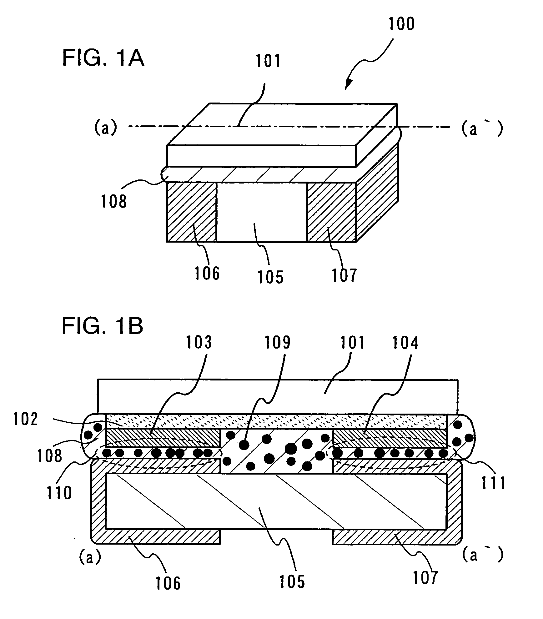
[0043]FIG. 1A is a perspective view for showing an optical sensor 100. The optical sensor 100 is composed of a plastic substrate 101 provided with a semiconductor element (not shown in the figure), a heat-resistant substrate 105 (hereinafter, an interposer) provided with conductive films 106 and 107 at both ends portions of the heat-resistant substrate, and an adhesive agent 108 for bonding the plastic substrate 101 to the heat-resistant substrate 105 together.

[0044]FIG. 1B is a cross-sectional view taken along line (a)-(a′) of FIG. 1A. A semiconductor element 102 is formed over a plastic substrate 101, and electrode terminals 103 and 104 that are leading out electrodes of the semiconductor element are formed. In this embodiment mode, the semiconductor element serves as a light receiving portion. Moreover, connection terminals (side electrodes) 106 and 107 are formed at both ends of th...

embodiment mode 2

[0060] In this embodiment mode, a method for mounting of an optical sensor shown in Embodiment Mode 1 over a wiring substrate is described with reference to FIG. 2.

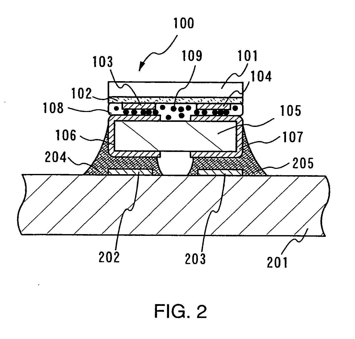
[0061]FIG. 2 is a cross-sectional view for showing that an optical sensor 100 is mounted over a wiring substrate 201. An interposer 105 in which connection terminals (side electrodes) 106 and 107 are formed and a semiconductor element 102 (in this embodiment mode, a light receiving portion) that is formed on a plastic substrate 101 are bonded to each other via an anisotropic conductive adhesive agent 108. Moreover, electrode terminals 103 and 104 of the light receiving portion and the connection terminals (side electrodes) 106 and 107 that is formed at edge portions of the interposer is electrically connected to each other via a conductive particle 109 that is included in the anisotropic conductive adhesive agent 108.

[0062] In addition, connection terminals (side electrodes) 106 and 107 that are formed on the interposer...

embodiment mode 3

[0069] In this embodiment mode, a light receiving portion of an optical sensor that is a semiconductor element shown in embodiment mode 1 and 2 is described with reference to FIG. 3 to FIG. 4B.

[0070]FIG. 3 is a cross-sectional view for showing an optical sensor 300 of the present invention. A first electrode 311, a light receiving portion 302, and a second electrode 312 are formed over a plastic substrate 301. The first electrode is connected to a first electrode terminal 313, and the second electrode is connected to a second electrode terminal 314. The first electrode terminal 313 and the second electrode terminal 314 are electrically insulated with an interlayer insulating film 315 therebetween. The first electrode terminal and the second electrode terminal are terminals for connecting to a wiring on a wiring substrate.

[0071] In the case that light is incident from the plastic substrate 301 side, the first electrode is formed from a conductive film that ohmic contact with a semi...


PUM


Abstract

The present invention provides a semiconductor device having a structure that can be mounted on a wiring substrate, as for the semiconductor device formed over a thin film-thickness substrate, a film-shaped substrate, or a sheet-like substrate. In addition, the present invention provides a method for manufacturing a semiconductor device that is capable of raising a reliability of mounting on a wiring substrate. One feature of the present invention is to bond a semiconductor element formed on a substrate having isolation to a member that a conductive film is formed via a medium having an anisotropic conductivity.

Description

BACKGROUND OF THE INVENTION [0001] 1. Field of the Invention [0002] The present invention relates to a semiconductor device that is thin and lightweight, and a manufacturing method thereof. Specifically, a semiconductor device using a substrate having a thin thickness or a film-shaped substrate, and a manufacturing method thereof. [0003] 2. Description of the Related Art [0004] In recent years, cellular phones spread with the progress of communication technology. It is expected that cellular phones transmit moving image and more communication are expected more in future. On the other hand, laptop computers for mobile have been produced due to the weight saving. A large number of personal digital assistances referred to as PDA that begin from electronic notebook have been produced, and diffused. Moreover, most of such personal digital assistances are each mounted with a flat panel display by the development of display devices. [0005] In such a display device, the brightness around th...

Claims


Application Information

Patent Timeline
Patent Type & Authority Applications(United States)
IPC IPC(8): H01L21/00H01L21/60H01L23/12H01L27/14H01L23/498H01L27/146H01L31/0203H01L31/04H01L31/10
CPCH01L23/49805H01L24/29H01L24/32H01L24/83H01L31/0203H01L2224/2929H01L2924/01078H01L2924/01079H01L2924/09701H01L2924/07811H01L2224/293H01L2224/83851H01L2924/3512H01L2924/00H01L2924/00014H01L2924/12042H01L2924/12036H01L2924/14H01L21/60
Inventor NISHI, KAZUOADACHI, HIROKIKUSUMOTO, NAOTOSUGAWARA, YUUSUKETAKAHASHI, HIDEKAZUYAMADA, DAIKIHIURA, YOSHIKAZU
Owner SEMICON ENERGY LAB CO LTD
Why Eureka
Try Eureka