Electro-optical panel, sealing member, electro-optical panel manufacturing method, self-emission panel, self-emission panel manufacturing method, and sealing member for use in self-emission panel

a manufacturing method and electrooptical technology, applied in the manufacture of cold cathode, electric discharge tube/lamp, electrooptical system, etc., can solve the problems of difficult to solve the above problems, lead-out area a has to be made inevitably large, and the breakage of the support substrate becomes even worse. , to achieve the effect of less breakage and adequate strength

Inactive Publication Date: 2006-11-30
TOHOKU PIONEER CORP
View PDF0 Cites 18 Cited by
  • Summary
  • Abstract
  • Description
  • Claims
  • Application Information

AI Technical Summary

Benefits of technology

[0019] The present invention is to solve the aforementioned problems and it is an object of the invention to provide a support structure having an adequate strength to meet the requirement of making a thin electro-optical panel, ensuring a structure capabl

Problems solved by technology

In particular, when adopting the COG shown in the drawing, a relatively large space is required to connect or mount driving means such as circuit elements or the like, so that the lead-out area A has to be made inevitably large.
This, however, causes a problem in which the support substrate is easy to break at the inner end position A0, and the breakage of support substrate becomes even worse if the support substrate is made still thinner.
However, once there is an external force which is equal to or larger than an adhesion strength combining together the adhesion resin J5 and the sealing member J2, the support substrate will be broken at the inner end position A0, making it difficult to solve the aforementioned problem.
It is known that if a self-emission panel is an organic EL panel, when organic EL devices essential for forming the self-emission section are exposed to the outside atmosphere

Method used


Image

  • Electro-optical panel, sealing member, electro-optical panel manufacturing method, self-emission panel, self-emission panel manufacturing method, and sealing member for use in self-emission panel
  • Electro-optical panel, sealing member, electro-optical panel manufacturing method, self-emission panel, self-emission panel manufacturing method, and sealing member for use in self-emission panel
  • Electro-optical panel, sealing member, electro-optical panel manufacturing method, self-emission panel, self-emission panel manufacturing method, and sealing member for use in self-emission panel

Examples


Embodiment Construction

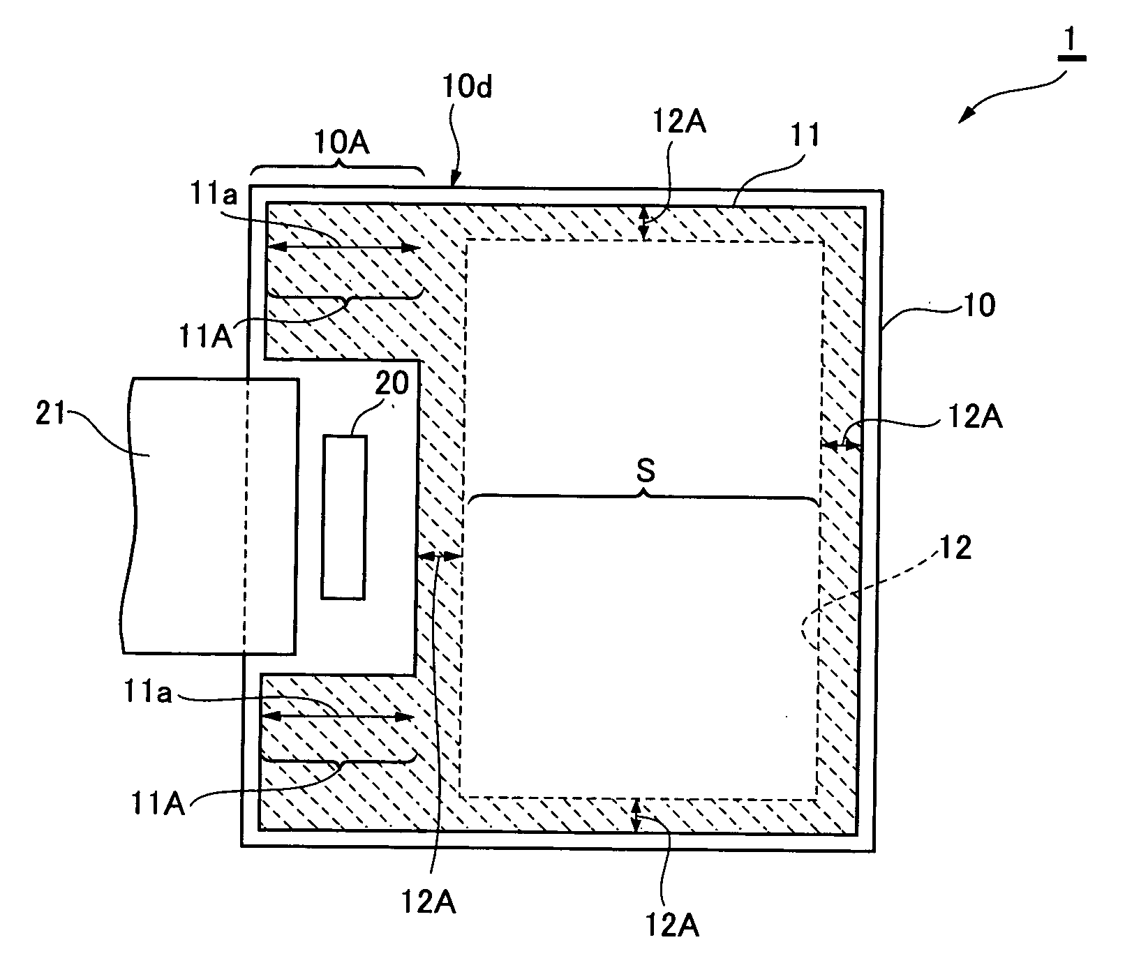
[0047] Hereafter, preferred embodiments of the present invention will be described with reference to the accompanying drawings. FIGS. 3(a) and 3(b) are explanatory views showing an electro-optical panel formed according to one embodiment of the present invention (FIG. 3(a) is a plan view and FIG. 3(b) is a side view). As shown, the electro-optical panel 1 has a basic structure in which a sealing area S including an electro-optical functional section is formed between a pair of mutually facing members. Here, so-called mutually facing members may include a support substrate 10 and a sealing member 11 which will be explained later, or a pair of mutually facing flat support substrates.

[0048] Here, one of a pair of mutually facing members comprises a support substrate 10 which includes a lead-out area 10A containing an area provided with a lead-out wiring (not shown) extending from the sealing area S and connecting or mounting the driving means (such as IC chip 20 and flexible substrate...


PUM


Abstract

It is an object of the present invention to provide an improved structure having an adequate strength to satisfy a requirement of making a thin electro-optical panel. The electro-optical panel forms a sealing area having an electro-optical functional section between the support substrate and the sealing member. The support substrate has a lead-out area containing an area for forming lead-out wiring extending from the sealing area and for connecting or mounting the driving means (IC chip, flexible substrate and the like) to the lead-out wiring. The sealing member has protruding reinforcement sections protruding from the sealing area S on to the lead-out area. The support substrate and the sealing member are bonded together through an adhesive layer, thereby forming an adhesive area surrounding the sealing member. It is another object of the present invention to provide an improved process of producing a plurality of self-emission panels formed by cutting a mother panel into a plurality of unit panels, to prevent lead-out wiring portions from being wounded during the cutting process, thereby improving the yield of production. A further object of the invention is to improve the efficiency of inspection step, thereby improving the productivity of manufacturing process. A mother self-emission panel comprises a mother support substrate having formed thereon a plurality of self-emission sections, and a mother sealing member having arranged thereon a plurality of sealing sections corresponding to the plurality of self-emission sections. When the mother support substrate and the mother sealing member are bonded together, a plurality of sealing areas will be formed to seal the plurality of self-emission sections corresponding to the plurality of sealing sections. The mother support substrate has a plurality of lead-out areas having formed thereon a plurality of lead-out wiring portions extending from the plurality of self-emission sections to the outsides of the sealing areas. The mother sealing member has a plurality of hole processing portions for exposing the lead-out wiring portions.

Description

BACKGROUND OF THE INVENTION [0001] The present invention relates to an electro-optical panel, a sealing member and a method of manufacturing the electro-optical panel. [0002] The present application claims priority from Japanese Application No. 2005-151298, the disclosures of which are incorporated herein by reference. [0003] Electro-optical panels represented by EL (Electroluminescent) display panel, PDP (Plasma Display Panel), FED (Field Emission Display) panel or liquid crystal display panel are usually adopted in various kinds of electronic apparatus, serving as a flat-panel display, an illumination member or the like. In particular, an organic EL panel can of course perform a color-displaying capable of obtaining a desired brightness efficiency at various colors RGB, and is characterized in that its drive voltage is as low as several to several tens of volts, provides a high visibility even when viewed from an inclined angle, and exhibits a high velocity response with respect t...

Claims


Application Information

Patent Timeline
IPC IPC(8): H01J9/26
CPCH01J5/24H01J5/32H01J9/261H01J9/32H01J17/183H01J17/186H01L2251/566H01J2329/90H01L27/3276H01L27/3288H01L51/5237H01L51/56H01J2329/867H10K59/179H10K59/131H10K50/841H10K71/851H10K71/00
Inventor AITA, TOSHIHARU
Owner TOHOKU PIONEER CORP
Why Eureka
Try Eureka