Polarizer based on a nanowire grid

a polarizer and nanowire technology, applied in the field of nanowire grids, can solve the problems of difficult to create wire grid structures with a period of 150 nm or less, and the cost associated with the use of tools designed for these applications is considered very significan

Active Publication Date: 2006-12-07
WOSTEC
View PDF15 Cites 40 Cited by
  • Summary
  • Abstract
  • Description
  • Claims
  • Application Information

AI Technical Summary

Benefits of technology

[0007] A variety of optoelectronic applications can benefit from the development of ef

Problems solved by technology

However, the cost associated with the use of the tools designed for these applications is considered very significant.
The existing approach and tools make it difficult to scale the production from smaller semiconductor wafer sizes to larger area substrates (such as glass sheets or plastic).
In addition, the existing approach makes it is very difficult to create wire grid structures with a period of 150 nm or less.
However, experiments using nanostru

Method used


Image

  • Polarizer based on a nanowire grid
  • Polarizer based on a nanowire grid
  • Polarizer based on a nanowire grid

Examples


Embodiment Construction

[0019] Detailed descriptions of the preferred embodiments are provided herein. It is to be understood, however, that the present inventions may be embodied in various forms. Therefore, specific implementations disclosed herein are not to be interpreted as limiting.

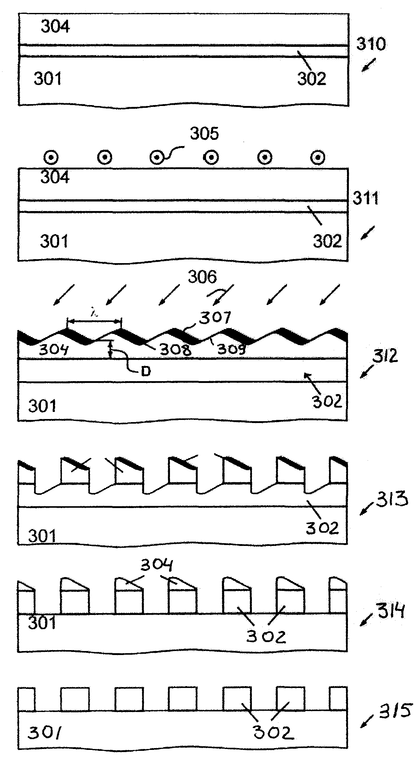
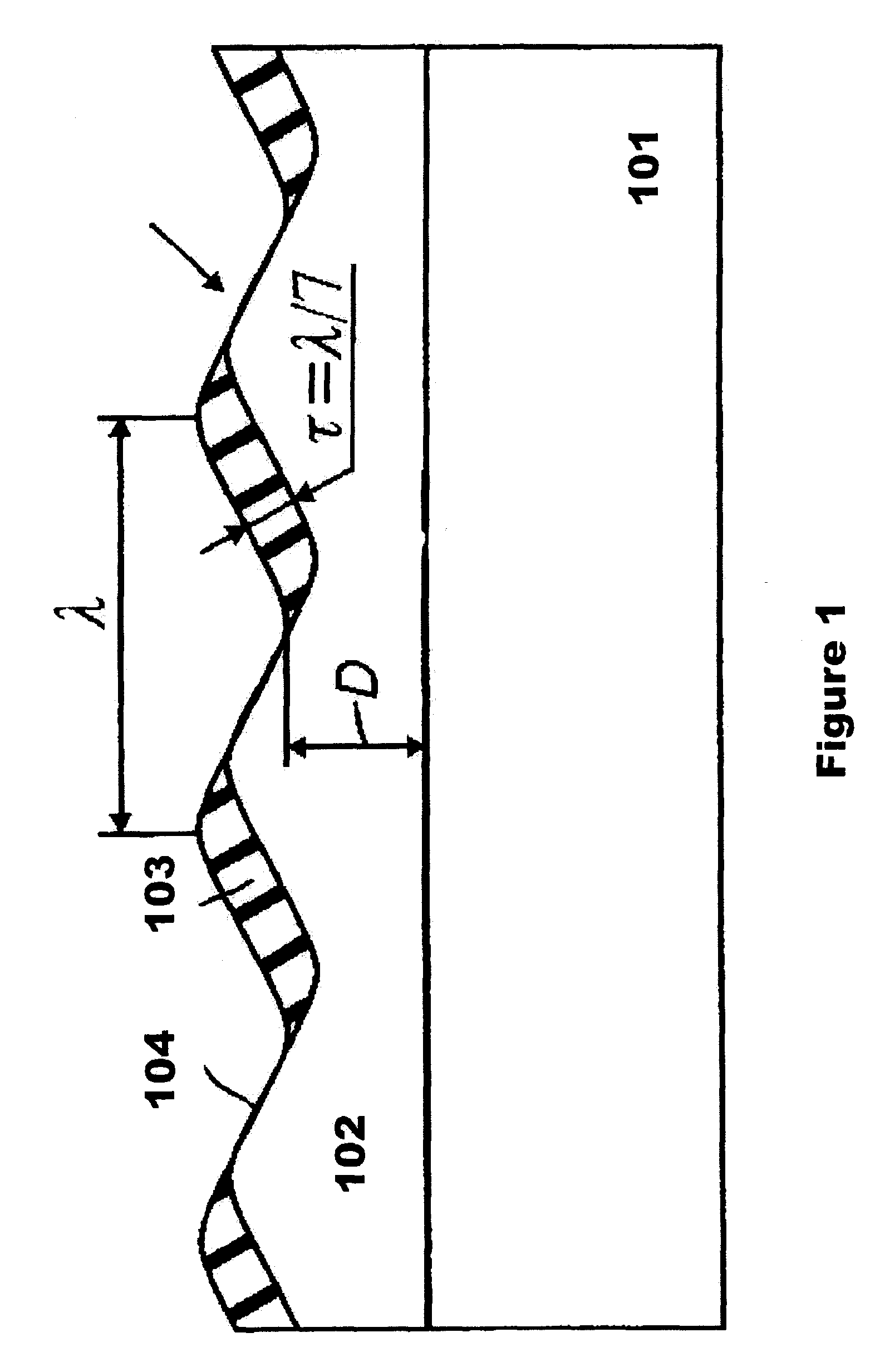
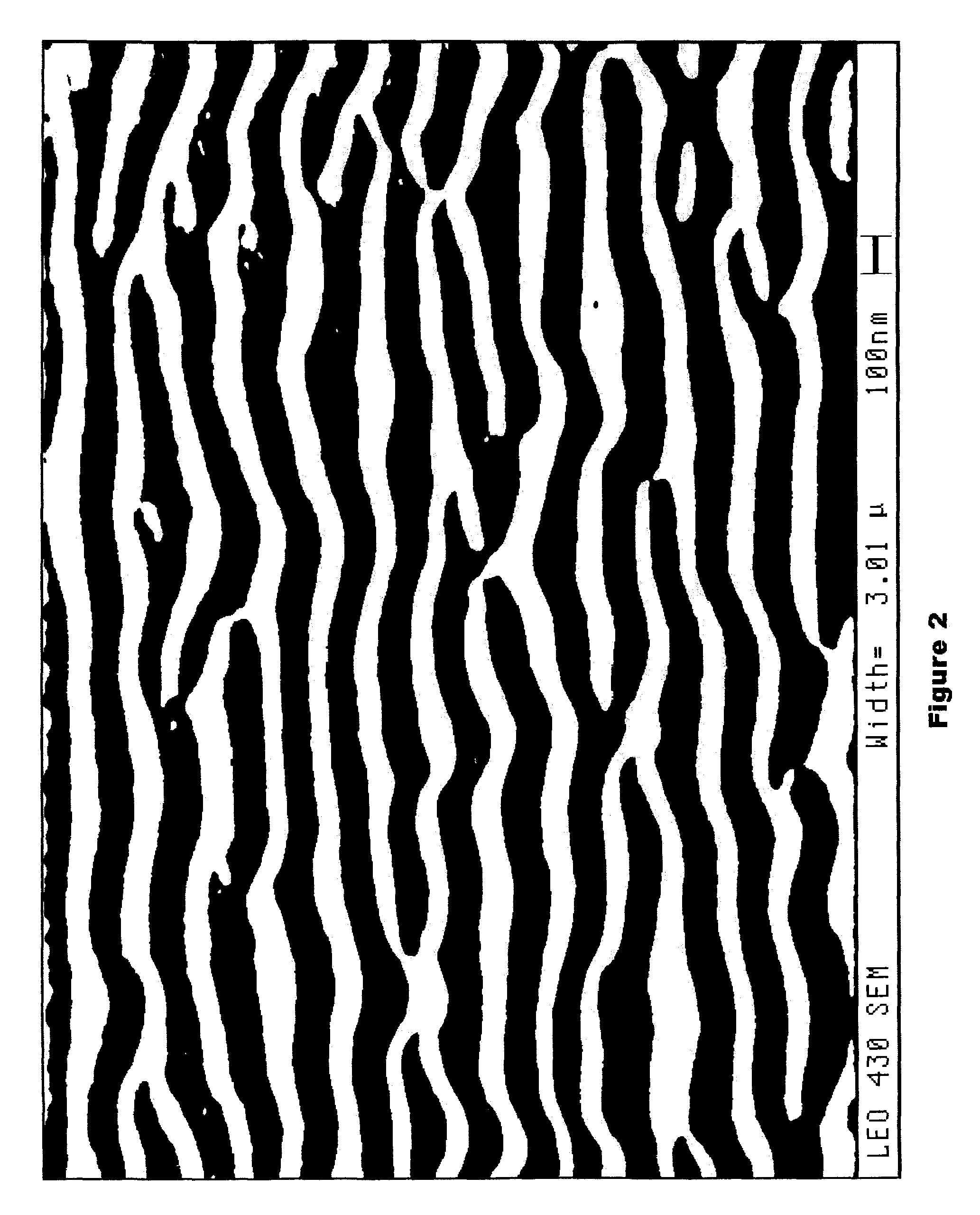
[0020] A preliminary treatment (a treatment applied before the sputtering step) of the amorphous silicon layer, causing a uniform anisotropic stress within this layer, considerably increases the degree of nanostructure pattern orientation (i.e., its coherency.)

[0021] According to this approach, the layer in which the wave ordered structure (WOS) will be built is manufactured so that there is a substantially uniform mechanical anisotropic stress. The stress can be induced during the deposition process by applying an anisotropic surface treatment or additional irradiation, or after the deposition, before or simultaneously with ion bombardment.

[0022] In one preferred embodiment, an oriented polishing (a polishing of the su...


PUM


Abstract

The preferred embodiment provides for development and use of an array of nanowires with a period smaller then 150 nm for applications such as an optical polarizer. To manufacture such structures the preferred embodiment employs a hard nanomask. This nanomask includes a substantially periodic array of substantially parallel elongated elements having a wavelike cross-section.

Description

RELATED APPLICATIONS [0001] This application claims the benefit of U.S. Provisional Patent Application Ser. No. 60 / 686,495, filed Jun. 1, 2005, and is a continuation-in-part of U.S. patent application Ser. No. 11 / 385,355, filed Mar. 21, 2006, which is a national phase application of PCT / RU2004 / 000396, filed Oct. 8, 2004, which claims the benefit of Russian Application No. 200329927, filed Oct. 10, 2003, all of which are hereby incorporated by reference in their entirety.FIELD OF THE INVENTION [0002] The invention relates to non-lithographic methods for manufacturing devices such as a polarizer, comprised of a grid of metal conductors, located on the surface of an optically transparent substrate or embedded into the substrate, by filling grooves on the substrate with metal. It also generally relates to methods and devices for forming periodic wire grids with a period of 150 nm or less. BACKGROUND OF THE INVENTION [0003] Wire grid polarizers are widely used in devices for graphic info...

Claims


Application Information

Patent Timeline
IPC IPC(8): B29D11/00G02B5/30
CPCB82Y20/00G02B5/3058Y10S438/974Y10S438/982Y10T428/249953Y10T428/249961
Inventor SMIRNOV, VALERY K.KIBALOV, DMITRY S.
Owner WOSTEC
Why Eureka
Try Eureka