Semiconductor wafer marking apparatus having marking interlock system and semiconductor wafer marking method using the same

a technology of semiconductor wafers and marking apparatuses, which is applied in the direction of semiconductor/solid-state device testing/measurement, manufacturing tools, lasers, etc., can solve the problems of changing the energy of laser beams, the conventional method is disadvantageous in cost and time, and the inability to detect marking defects during the marking process

Inactive Publication Date: 2006-12-07
SAMSUNG ELECTRONICS CO LTD
View PDF11 Cites 9 Cited by
  • Summary
  • Abstract
  • Description
  • Claims
  • Application Information

AI Technical Summary

Benefits of technology

[0016] The present invention provides a semiconductor wafer marking apparatus that maintains the energy of a laser beam radiated onto a wafer to form a uniform identification mark on the wafer, and that has a marking interlock system that terminates a malfunctioning marking operation.

Problems solved by technology

Such a marking defect cannot be detected during the marking process, but only after the subsequent manufacturing processes have been completed.
For this reason, the conventional method is disadvantageous in terms of costs and time.
Another potential cause of change in the energy of the laser beam is cooling water leakage in the pipe 90.
Consequently, the above-described marking defects cannot be prevented.

Method used


Image

  • Semiconductor wafer marking apparatus having marking interlock system and semiconductor wafer marking method using the same
  • Semiconductor wafer marking apparatus having marking interlock system and semiconductor wafer marking method using the same
  • Semiconductor wafer marking apparatus having marking interlock system and semiconductor wafer marking method using the same

Examples


Embodiment Construction

[0046] Hereinafter, the present invention will be described more fully with reference to the accompanying drawings, in which exemplary embodiments of the invention are shown. The invention may, however, be embodied in many different forms and should not be construed as being limited to the embodiments set forth herein; rather, these embodiments are provided so that this disclosure will be thorough and complete. In the drawings, like reference numerals denote like elements, and the sizes and thicknesses of layers and regions are exaggerated for clarity.

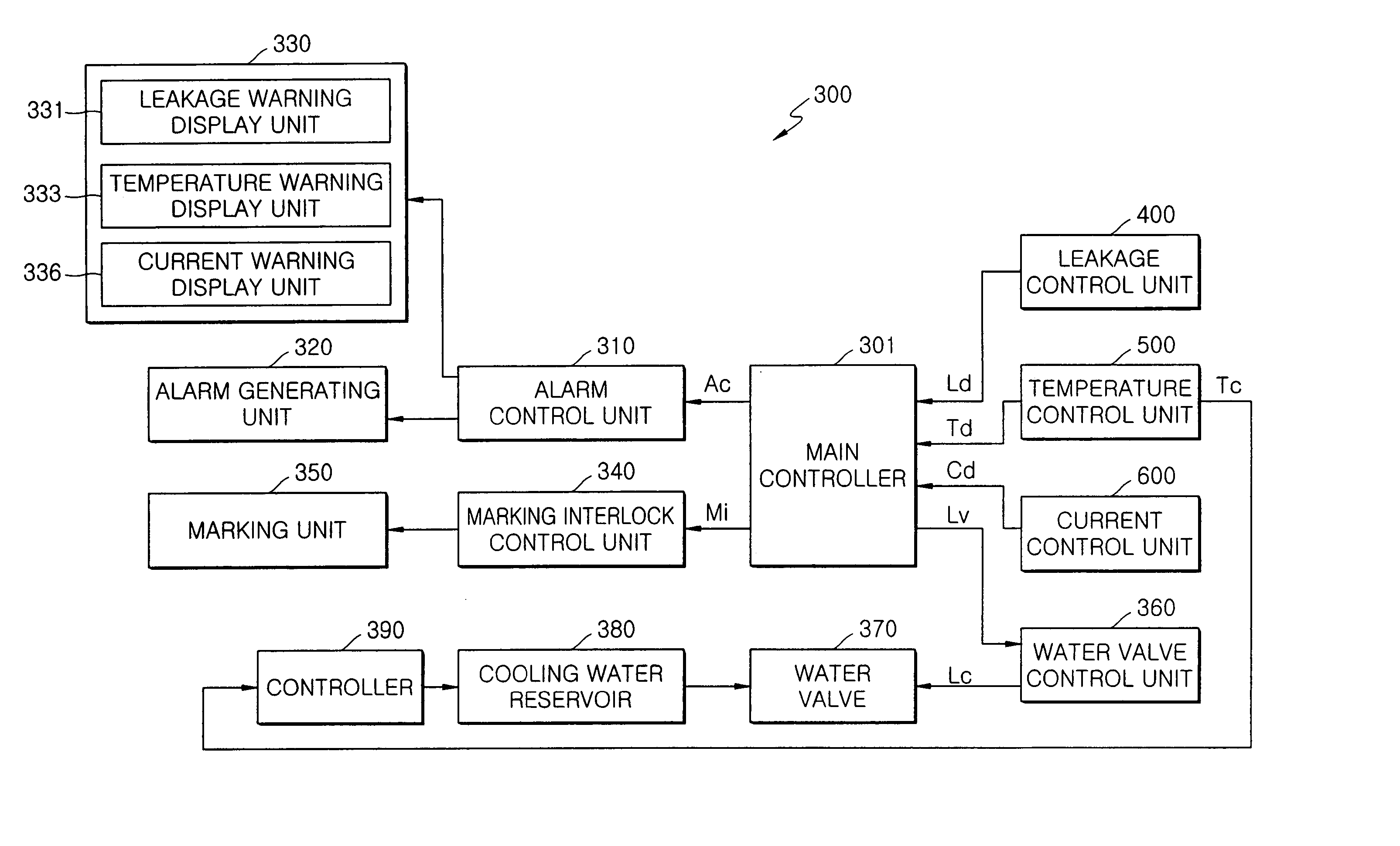
[0047]FIG. 4 is a schematic diagram of a semiconductor wafer marking apparatus 100 according to an embodiment of the present invention. FIG. 5 is a perspective view of a laser head unit 200 and a marking interlock system 300 of the semiconductor wafer marking apparatus 100 of FIG. 4, according to an embodiment of the present invention. Referring to FIGS. 4 and 5, the semiconductor wafer marking apparatus 100 includes the laser head un...


PUM

PropertyMeasurementUnit
energyaaaaaaaaaa
constant temperatureaaaaaaaaaa
temperatureaaaaaaaaaa

Abstract

In a semiconductor wafer marking apparatus having a marking interlock system and a semiconductor wafer marking method using the same, the semiconductor wafer marking apparatus includes a laser head unit including a flowcell having a laser radiation region on an upper surface thereof and a laser source radiating laser energy on the laser radiation region in response to an input current. An optical system focuses the laser energy radiated from the laser source to form a laser beam and radiates the laser beam on the semiconductor wafer. A cooling water reservoir stores cooling water. A pipe is disposed in the flowcell and connected to an inlet and an outlet of the cooling water reservoir. The cooling water flows through the pipe to maintain the laser radiation region of the flowcell at a constant temperature. A marking interlock system detects leakage of cooling water from the pipe, an abnormal temperature of the laser radiation region, and an abnormal input current supplied to the laser source, and generates a marking interlock signal to terminate a marking operation of the semiconductor wafer. A marking unit turns off the laser source to terminate the marking of the semiconductor wafer in response to the marking interlock signal generated by the marking interlock system.

Description

CROSS-REFERENCE TO RELATED PATENT APPLICATION [0001] This application claims priority to Korean Patent Application No. 10-2005-0048418, filed on Jun. 7, 2005, in the Korean Intellectual Property Office, the disclosure of which is incorporated herein in its entirety by reference. BACKGROUND OF THE INVENTION [0002] 1. Field of the Invention [0003] The present invention relates to a semiconductor wafer marking system, and more particularly, to a semiconductor wafer marking apparatus having a marking interlock system and a semiconductor wafer marking method using the same. [0004] 2. Description of the Related Art [0005] In general, photography, ion diffusion, etching, and deposition are repeatedly performed on a wafer when manufacturing a semiconductor device. A test process is then performed on the wafer following manufacturing of the semiconductor device to determine whether the wafer has defects. When the test process is completed, the wafer is cut in a scribing process, and is packa...

Claims


Application Information

Patent Timeline
Patent Type & Authority Applications(United States)
IPC IPC(8): H01L21/76H01L23/544B23K26/00H01L21/02H01S3/00
CPCB23K26/365H01L21/67109H01L21/67248H01L21/67253H01L2223/54493H01L23/544H01L2223/54406H01L2223/54453H01L21/67282H01L2924/0002B23K26/361H01L2924/00H01L22/00
Inventor LIM, KI-YOUL
Owner SAMSUNG ELECTRONICS CO LTD
Why Eureka
Try Eureka