Connector having an electronic element built therein without disturbing a characteristic impedance

a technology of electronic elements and connectors, which is applied in the direction of connection contact materials, fixed connections, coupling devices, etc., can solve the problems of signal degradation, difficulty in controlling impedance characteristics, and the amount of solder

Inactive Publication Date: 2006-12-07
JAPAN AVIATION ELECTRONICS IND LTD +1
View PDF5 Cites 35 Cited by
  • Summary
  • Abstract
  • Description
  • Claims
  • Application Information

AI Technical Summary

Benefits of technology

[0007] It is therefore an object of this invention to provide a connector capable of connecting an electronic element without disturbing a characteristic impedance.

Problems solved by technology

It is therefore difficult to control impedance characteristics and signal degradation may occur due to impedance mismatching.
The impedance characteristics depend upon the shape of a soldering portion and the amount of a solder and are unstable.
Further, a soldering step is required in a production process so that the connector is increased in cost.

Method used


Image

  • Connector having an electronic element built therein without disturbing a characteristic impedance
  • Connector having an electronic element built therein without disturbing a characteristic impedance
  • Connector having an electronic element built therein without disturbing a characteristic impedance

Examples


Embodiment Construction

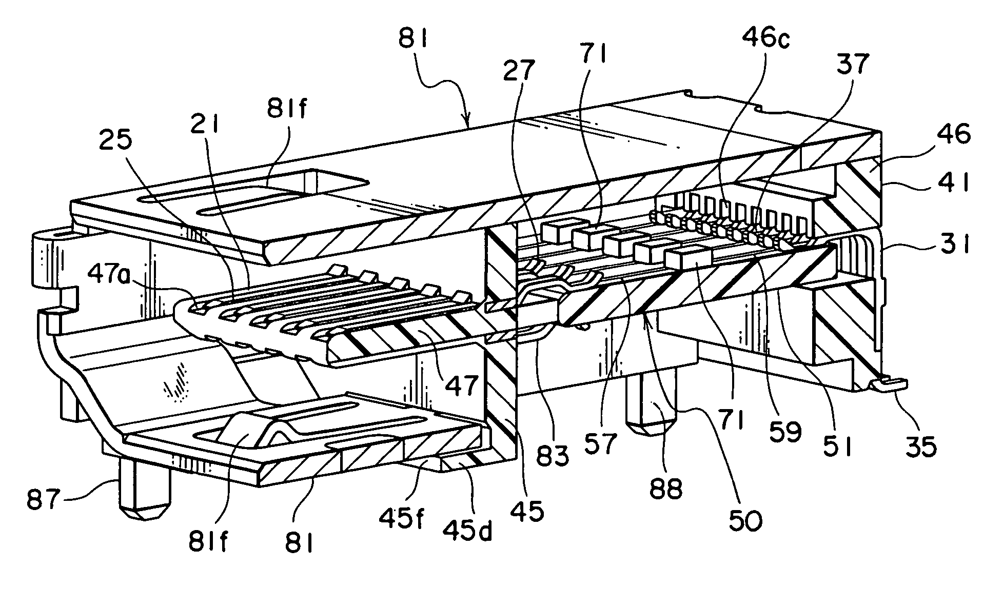
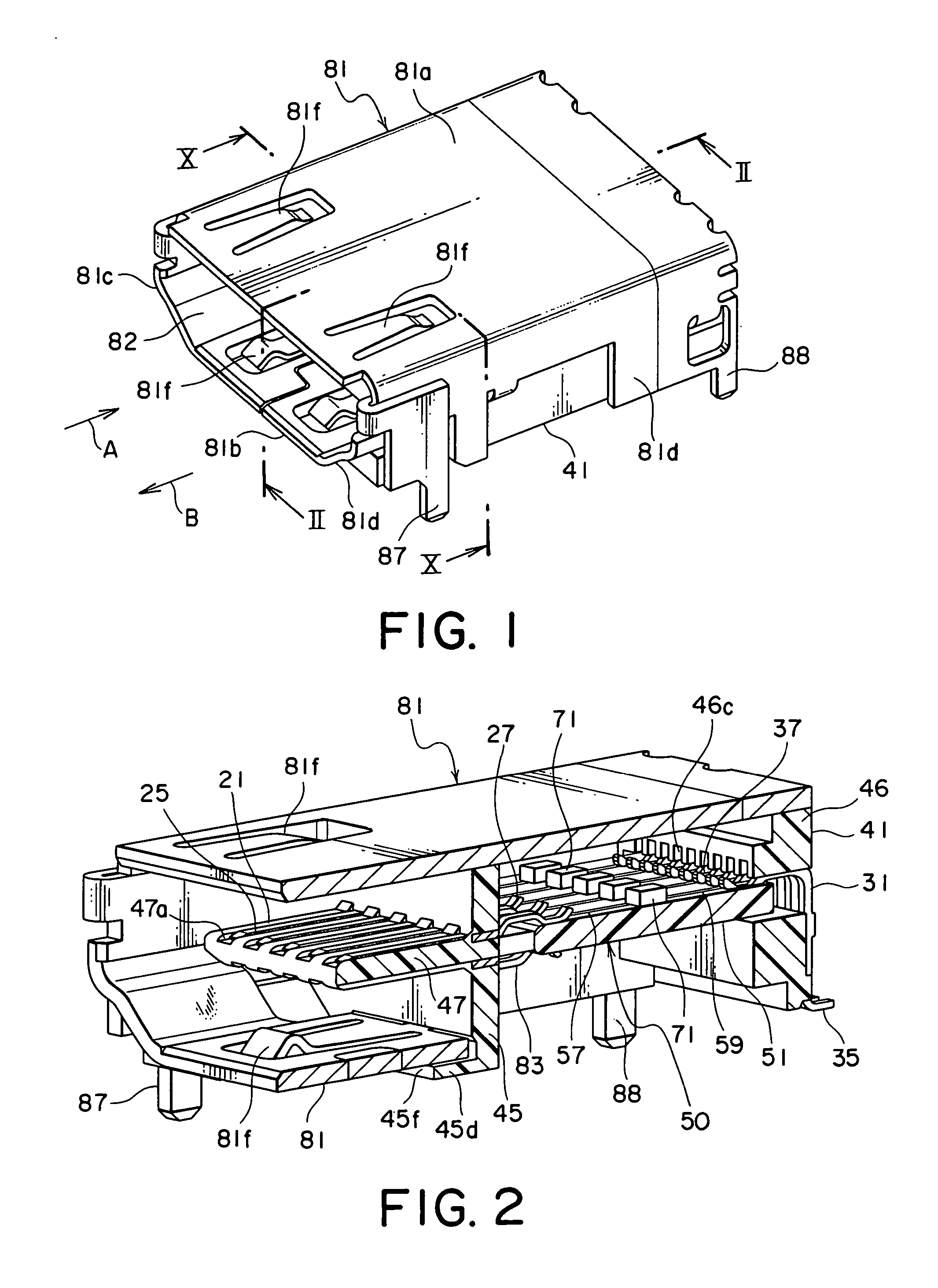
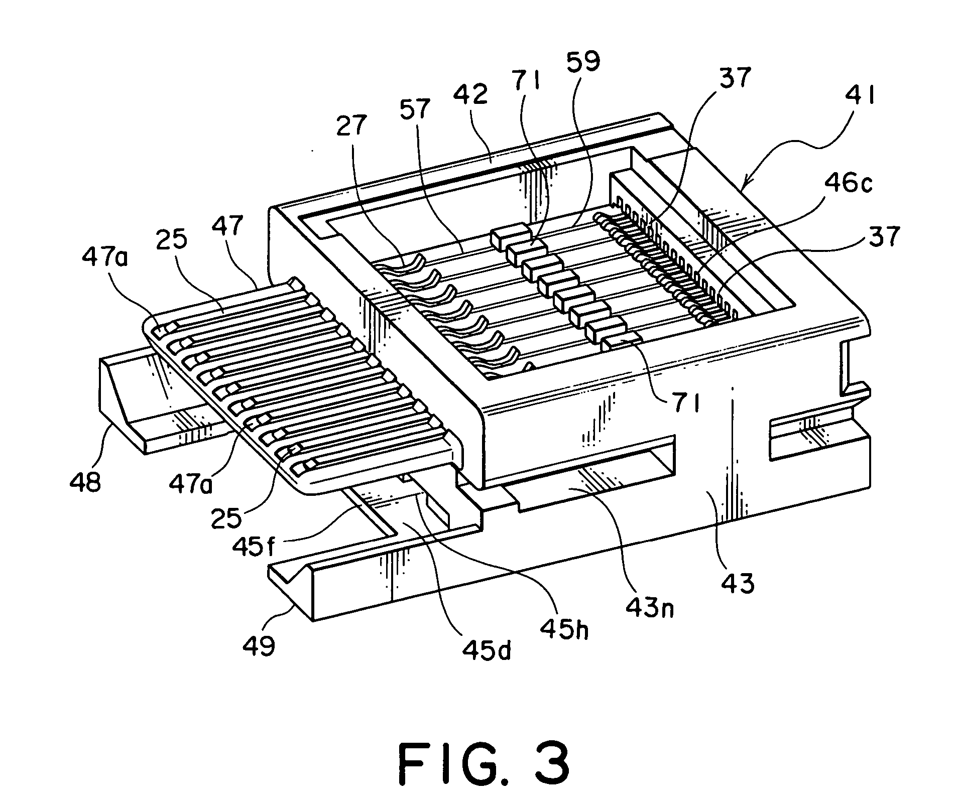
[0029] Referring to FIGS. 1 through 5, a whole of a connector according to an embodiment of this invention will be described.

[0030] The connector illustrated in the figures comprises a plurality of conductive first contacts 21, a plurality of conductive second contacts 31, an insulating housing 41 holding the first and the second contacts 21 and 31, a circuit board 51 disposed in the housing 41, and a metal shell 81 covering the housing 41 on its outside.

[0031] The first and the second contacts 21 and 31 are connected to the circuit board 51. Each of the first contacts 21 has a first holding portion 23 held by the housing 41, a first contacting portion 25 to be contacted with a mating connector (not shown), and a first elastic contacting portion 27 elastically contacted with the circuit board 51. Each of the second contacts 31 has a second holding portion 33 press-fitted into and held by a rear wall portion 46 of the housing 41, a second contacting portion 35 to be connected to a ...


PUM


Abstract

In a connector to be mounted to a connection object, an insulating housing holds a first and a second contact and has a receiving portion for receiving and holding a circuit board with an electronic element mounted thereon. The first contact has a first contacting portion to be contacted with a mating connector and a first elastic contacting portion brought into elastic contact with the circuit board. The second contact has a second contacting portion to be connected to the connection object and a second elastic contacting portion brought into elastic contact with the circuit board. Conductive first and conductive second connecting portions are disposed on the circuit board to be connected to the first and the second elastic contacting portions, respectively. In addition, a pair of ground patterns is disposed on the circuit board with the first and the second connecting portions interposed therebetween.

Description

[0001] This application claims priority to prior Japanese patent application JP 2005-161090, the disclosure of which is incorporated herein by reference. BACKGROUND OF THE INVENTION [0002] This invention relates to a connector having an electronic element built therein. [0003] For example, a connector of the type is disclosed in Japanese Unexamined Patent Application Publication (JP-A) No. 2000-252020. In the connector, a contact to be fitted to a mating connector is electrically connected to a cable through a substrate. The contact is inserted into a through hole of the substrate and connected to the through hole by soldering. By mounting electronic elements to the substrate, various functions are added to the connector. [0004] Another connector of the type is disclosed in Japanese Unexamined Patent Application Publication (JP-A) No. H6-151011. In the connector, a hybrid board with semiconductor components mounted thereto is built in a casing. A contact to be fitted to a mating con...

Claims


Application Information

Patent Timeline
Patent Type & Authority Applications(United States)
IPC IPC(8): H01R13/648H01R13/6474H01R13/66H01R13/719
CPCH01R12/57H01R12/725H01R23/688H01R13/6658H01R13/6585
Inventor TAKIMURA, YUTAISHI, KOUICHI
Owner JAPAN AVIATION ELECTRONICS IND LTD
Why Eureka
Try Eureka