Semiconductor pressure sensor

a pressure sensor and semiconductor technology, applied in the direction of fluid pressure measurement using inductance variation, measurement devices, instruments, etc., can solve the problems of unstable piezoresistive element electrical signal output, inability to obtain satisfactory sensitivity, and unstable measured values

Active Publication Date: 2006-12-14
MITSUBISHI ELECTRIC CORP
View PDF6 Cites 29 Cited by
  • Summary
  • Abstract
  • Description
  • Claims
  • Application Information

AI Technical Summary

Benefits of technology

[0015] According to the semiconductor pressure sensor of the present invention, it is possible to measure the pressure of the fluid to be measured in an accurate manner without being subject to the influence of a charged object in the fluid to be measured as well as an electric field from the outside.

Problems solved by technology

However, the fluid to be measured, which is an object for pressure measurement, generally has an electric charge whether it is a gas or a liquid, so when the fluid to be measured comes into contact with the diaphragm upon measurement of the pressure, the charged object is placed into contact with the diaphragm, too, whereby the resistance value of the piezoresistive element is caused to change under the influence of an electric field generated from this charged object, thus making an electric signal output from the piezoresistive element unstable.
However, the above-mentioned first patent document involves the following problem.
This increases the thickness of the diaphragm itself, so the amount of displacement of the diaphragm, which is caused to displace in accordance with the pressure of the fluid to be measured, becomes small, thus resulting in that a satisfactory level of sensitivity can not be obtained.
That is, when the silicon substrate has a reference potential, an electric field is necessarily generated between the shield film, which is zero potential, and the silicon substrate due to a potential difference therebetween, so the piezoresistive element is always subject to the electric field irrespective of the presence or absence of the charged object, as a result of which if the reference potential varies, the electric signal output from the piezoresistive element will also vary in accordance with the reference potential variation, thus making measured values unstable.

Method used


Image

  • Semiconductor pressure sensor
  • Semiconductor pressure sensor
  • Semiconductor pressure sensor

Examples


embodiment 1

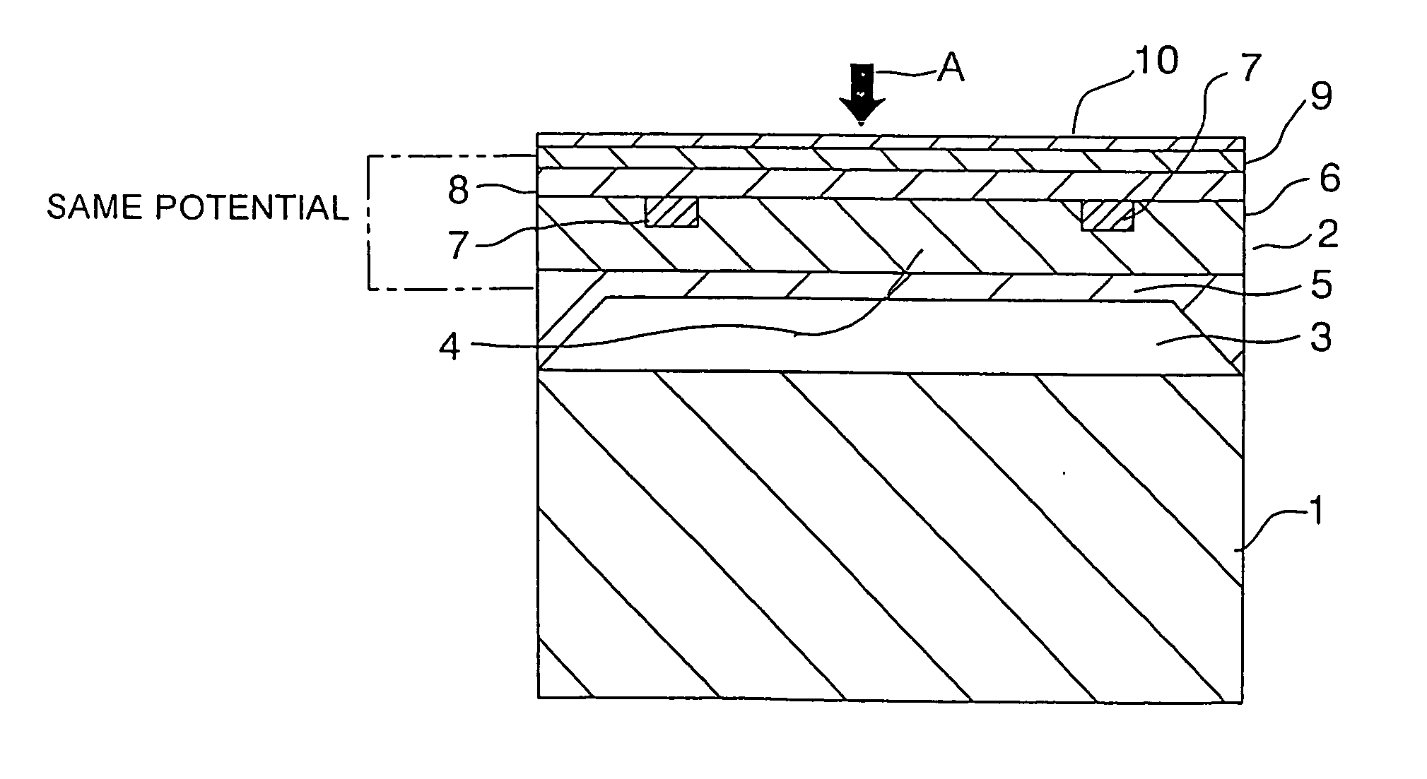
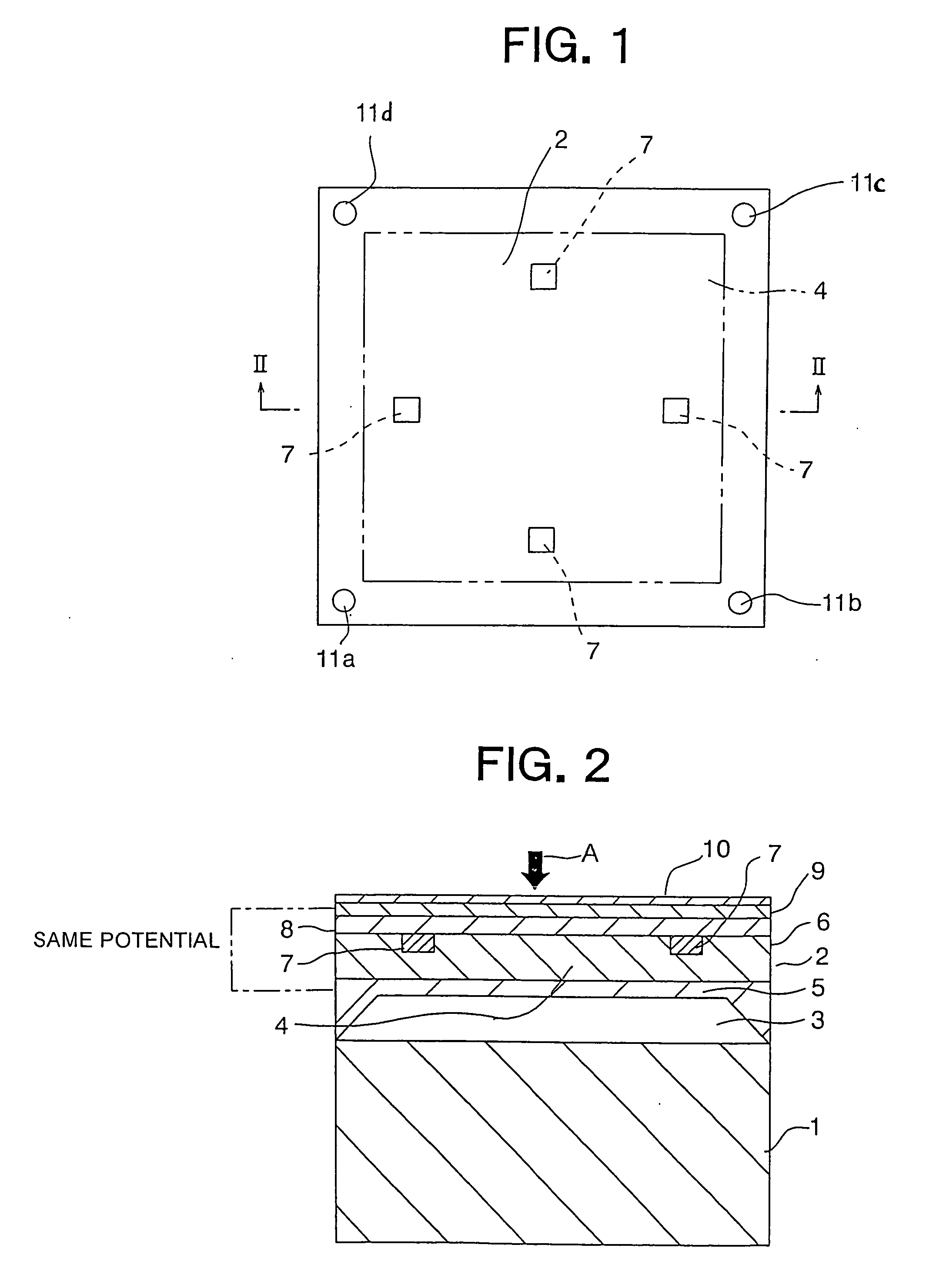
[0023]FIG. 1 is a cross sectional view that shows a semiconductor pressure sensor according to a first embodiment of the present invention, and FIG. 2 is a cross sectional arrow view along line II-II of FIG. 1.

[0024] In this semiconductor pressure sensor, a vacuum chamber or cavity 3 is formed between a glass substrate 1 and a sensor chip 2. The sensor chip 2 includes a diaphragm 4 which is adapted to be deformed in accordance with the pressure of a fluid to be measured, and a plurality of ( e.g., four in the illustrated example) pressure sensitive elements in the form of piezoresistive elements 7 formed through diffusion on the diaphragm 4. The four piezoresistive elements 7 are electrically connected with one another to constitute a Wheatstone bridge circuit. On a surface of the silicon substrate 6 at its side near the vacuum chamber 3, there is formed a reference potential film 5 that serves to apply a voltage to the Wheatstone bridge circuit. An insulating or dielectric oxide f...


PUM

PropertyMeasurementUnit
resistivityaaaaaaaaaa
pressureaaaaaaaaaa

Abstract

A semiconductor pressure sensor is not influenced by a charged object in a fluid to be measured or an electric field from the outside, so satisfactory sensitivity and accuracy can be ensured. The semiconductor pressure sensor is provided with a diaphragm 4 that responds to the pressure of the fluid to be measured. The diaphragm includes a silicon substrate with piezoresistive elements, which together constitute a bridge circuit, being embedded therein, and a shield film for electromagnetic shielding formed on a surface of the silicon substrate at a side thereof at which the fluid to be measured is in contact with the silicon substrate. The shield film is electrically connected to the silicon substrate so as to have the same potential as that of the silicon substrate.

Description

BACKGROUND OF THE INVENTION [0001] 1. Field of the Invention [0002] The present invention relates to a semiconductor pressure sensor equipped with a diaphragm that is moved in response to the pressure of a fluid to be measured for detecting a pressure such as, for example, the pressure in an intake manifold of an internal combustion engine, the internal pressure of a tank, etc. [0003] 2. Description of the Related Art [0004] In the past, there has been known a semiconductor pressure sensor that has a diaphragm formed on one surface of a silicon substrate with a piezoresistive element formed on the diaphragm. [0005] In this case, the diaphragm is caused to distort under the pressure of a fluid to be measured to change the resistance value of the piezoresistive element, whereby the pressure of the fluid to be measured can be detected by outputting an amount of change in the resistance value as an electric signal. [0006] However, the fluid to be measured, which is an object for pressur...

Claims


Application Information

Patent Timeline
Patent Type & Authority Applications(United States)
IPC IPC(8): G01L9/00
CPCG01L19/069G01L9/0055G01L9/06
Inventor FUJIMOTO, SEIZOHARA, TAKAFUMITARUYA, MASAAKI
Owner MITSUBISHI ELECTRIC CORP
Why Eureka
Try Eureka