NAND type flash memory array and method for operating the same

a technology of flash memory array and method, which is applied in the direction of digital storage, instruments, semiconductor devices, etc., can solve the problems of low random access characteristic, slow programming speed, and relative weak point of integration, so as to improve the characteristics of the reading operation of the memory cell, reduce the effect of program disturbance and improve the efficiency of self-boosting

Active Publication Date: 2006-12-14
SEOUL NAT UNIV R&DB FOUND +1
View PDF10 Cites 23 Cited by
  • Summary
  • Abstract
  • Description
  • Claims
  • Application Information

AI Technical Summary

Benefits of technology

[0017] Another aspect of the present invention is to provide a NAND type flash memory array on an SOI substrate, improve characteristics of the reading operation of a memory cell and connect the conduction path, which is formed under a shallow junction of memory cells, to the body biasing contact region. This enables all memory cells with one contact terminal, which is formed on the body biasing contact region, to body bias and do the erasing operation.
[0018] A further aspect of the present invention is to provide a technology that reduces a program disturbance effectively by raising the efficiency of self-boosting on the programming operation with the lower voltage VPASS than a conventional voltage.

Problems solved by technology

However, it has a relative weak point for integration.
On the contrary, in a NAND type flash memory, the speed of programming is slow due to an F-N tunneling mechanism, and the random access characteristic is not good.
However, a NAND type flash memory array with FDSOI has difficulty in applying an appropriate body bias to the fully depleted body region and it makes erasing a memory cell difficult.
However, there is still slight program disturbance, and it is a factor which limits the number of programs in a NAND type flash memory array.
When the voltage VPASS is too low, the self-boosting is ineffective and cell C is interfered.
When the voltage VPASS is too high, cell B is interfered.
This interference does harm to the reliability of the memory cell, and it is a factor which limits the number of programs.
However, in a conventional NAND type flash memory array with an SOI structure, it is impossible to erase a flash memory as in TABLE 1, because a bulk bias is not applied.
If the erasing operation is attempted by applying a body voltage to a bulk under the insulator, the very high voltage, higher than the usual voltage, should be applied to it, due to a low efficiency of the body voltage transmitted to the channel by the small capacitance of the insulator.
However, characteristics of the reading and programming operation become just the same as an array which is manufactured with a bulk structure, and so there is no usefulness for the SOI substrate.

Method used


Image

  • NAND type flash memory array and method for operating the same
  • NAND type flash memory array and method for operating the same
  • NAND type flash memory array and method for operating the same

Examples


Embodiment Construction

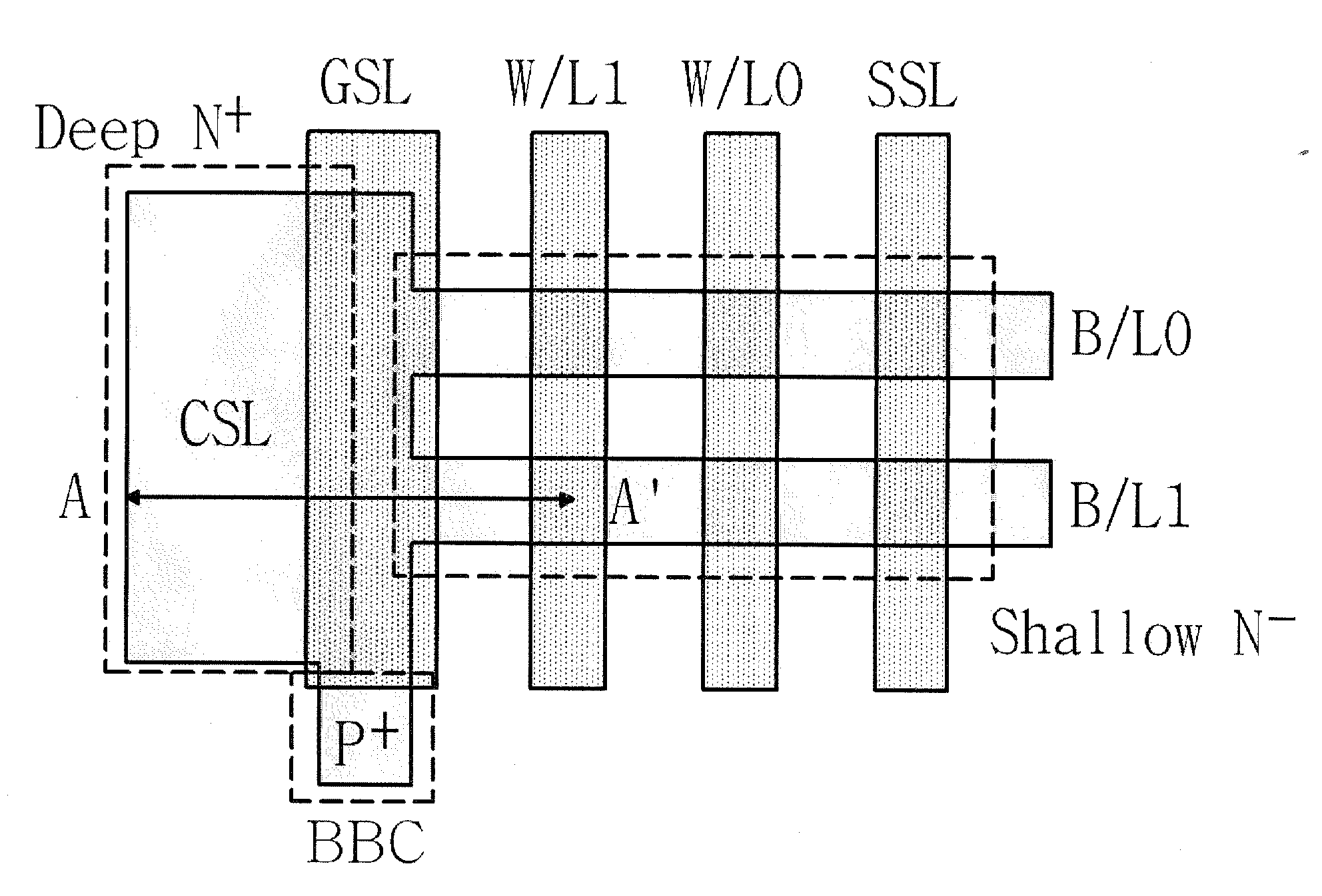
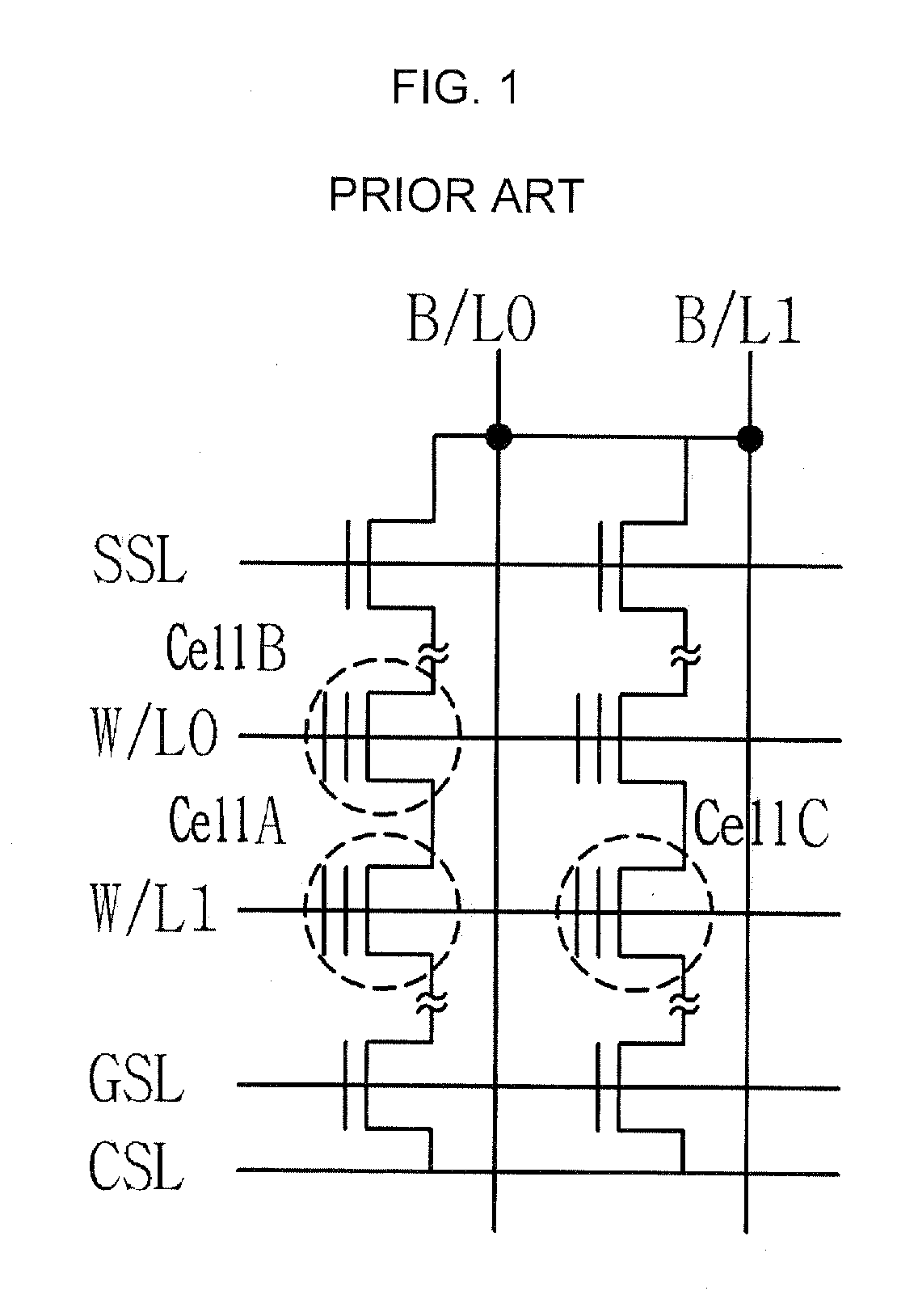
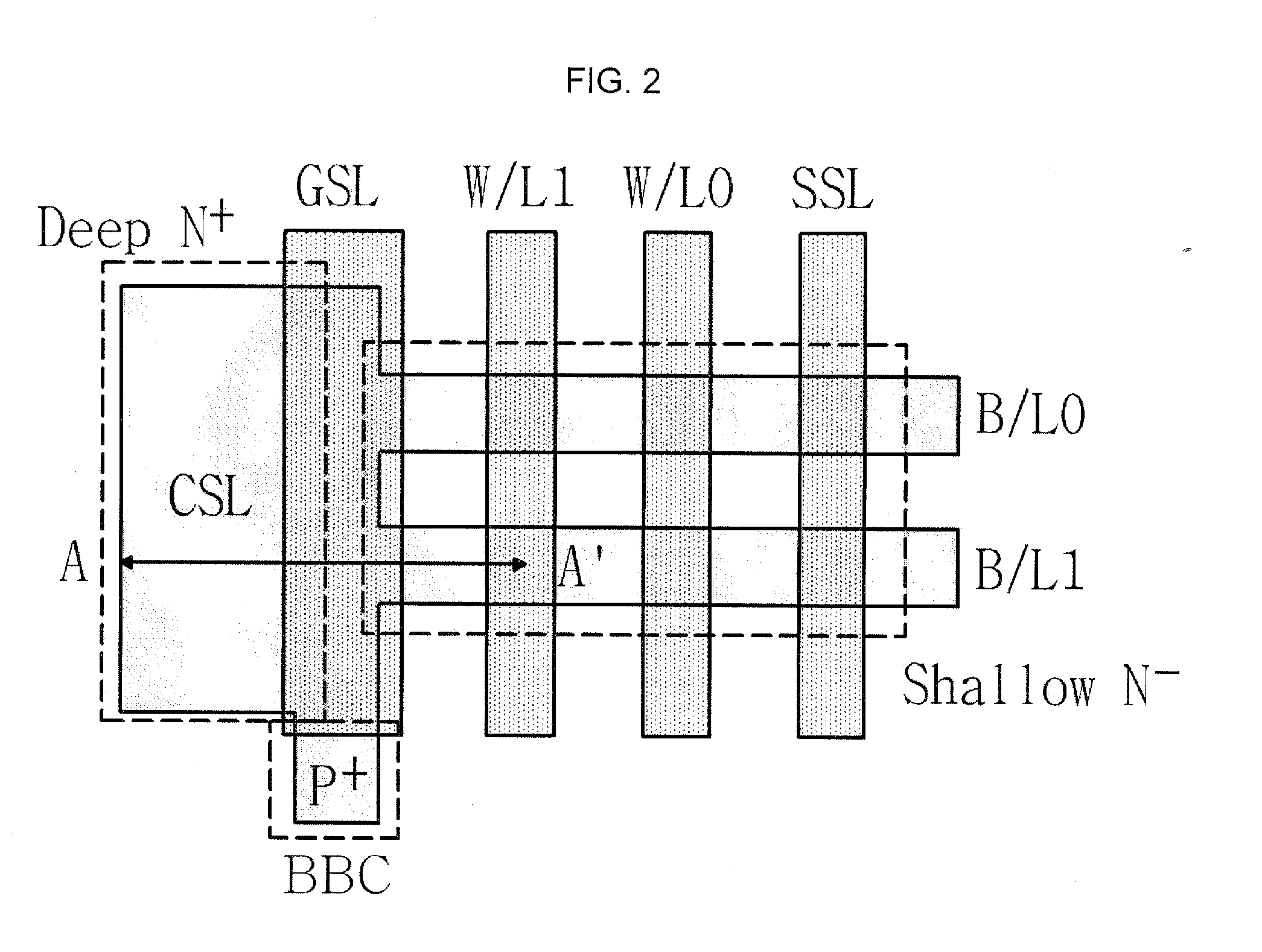
[0027] To accomplish objectives of the present invention, a NAND type flash memory array includes one or more bit lines on an SOI substrate; a first selective gate line arranged vertically to the bit lines; a plurality of word lines arranged vertically to the bit lines; a second selective gate line arranged vertically to the bit lines; a common source line arranged vertically to the bit lines; and a plurality of memory cells connected in series with a first selective transistor and a second selective transistor along each bit line, wherein the NAND type flash memory array includes a body biasing contact region which is connected to an active region on the lower part of one side of the second selective gate line.

[0028] A detailed description of preferred embodiments of a NAND type flash memory array of the invention is provided with respect to the accompanying drawings. It must be comprehended that the following preferred embodiments are exemplary only to help understand the present...


PUM


Abstract

A NAND type flash memory array which is composed of a plurality of memory cells with a shallow junction on an SOI substrate to make the body region depleted fully when each channel of the memory cells is turned on is provided. The invention improves the efficiency of a reading operation, enables an erasing operation on the SOI structure and enables use of a low voltage VPASS instead of a high voltage VPASS, which is used for a programming operation in a conventional NAND type flash memory array, and therefore it diminishes programming disturbance more effectively than a conventional array.

Description

CROSS-REFERFNCE TO RELATIED APPLICATION [0001] This application claims priority under 35 U.S.C. § 119 of Korean Patent Application 2005-0050108 filed on Jun. 11, 2005, the entire contents of which are hereby incorporated by reference. BACKGROUND [0002] 1. Technical Field [0003] The present invention relates to a NAND type flash memory array and a method for operating the same, and more particularly to a NAND type flash memory array with a cell structure which is doped with shallow junction on fully depleted silicon on insulator (FDSOI) and a method for operating the same. [0004] 2. Description of Related Art [0005] As the mobile and multi-media industry has been developed recently, a demand for flash memory has been increasing. [0006] Now, an application of flash memory enables one to store and update at any time system BIOS such as networking apparatuses (router, hub and so on), mobile phones and PDAs (personal digital assistants) and flash memory is a highly marketable product as ...

Claims


Application Information

Patent Timeline
Patent Type & Authority Applications(United States)
IPC IPC(8): G11C16/04
CPCH01L27/115G11C16/0483H10B69/00G11C16/0408
Inventor PARK, BYUNG-GOOKKIM, TAE-HOONPARK, IL HAN
Owner SEOUL NAT UNIV R&DB FOUND
Why Eureka
Try Eureka